


Part Number: DP83822I
Hi expert,
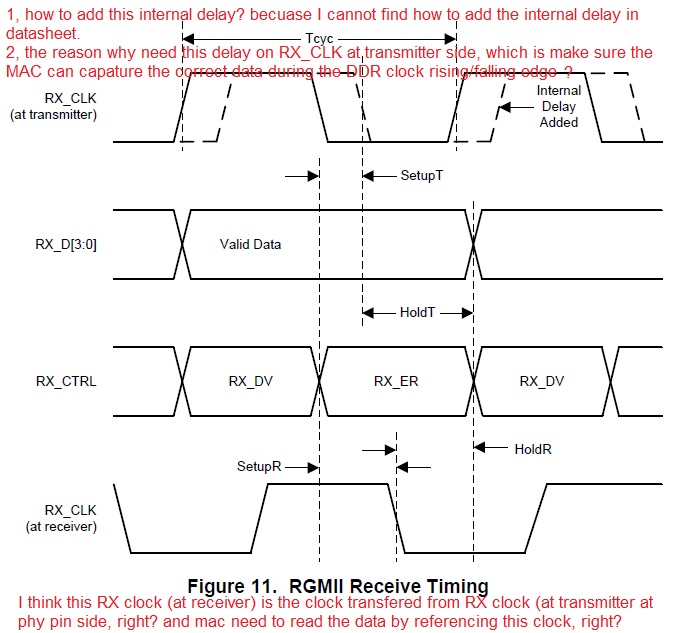
I would like to ask a question about the RGMII mode in DP83822I, you can see the figure 11 in datasheet.
1, how to add this internal delay if customer's pcb design use the equal line layout?
2, in below figure: what's the main reason for adding this delay? i am thinking when RX_CLK (at transmitter) which cannot be used as the reference DDR clock for data transmission,right?
3, so customer have to add the delay when RX clock going out from the PHY, such as the dot line clock in RX_CLK(at transmitter) waveform?
4, what's the meaning of the RX_CLK(at receiver) in below figure?
Best Regards
Iven Xu
