This thread has been locked.

If you have a related question, please click the "Ask a related question" button in the top right corner. The newly created question will be automatically linked to this question.

TCA9545A: No response on Channel 0-3 side

Part Number: TCA9545A
Other Parts Discussed in Thread: AM5718, LM63LM64LM96X63EVM, LM96063, PCA9545A

Hi,

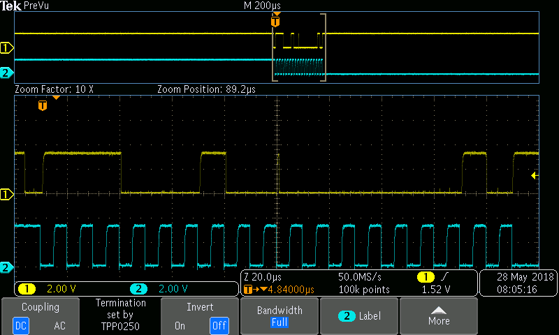
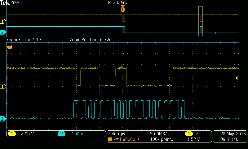
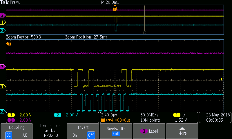
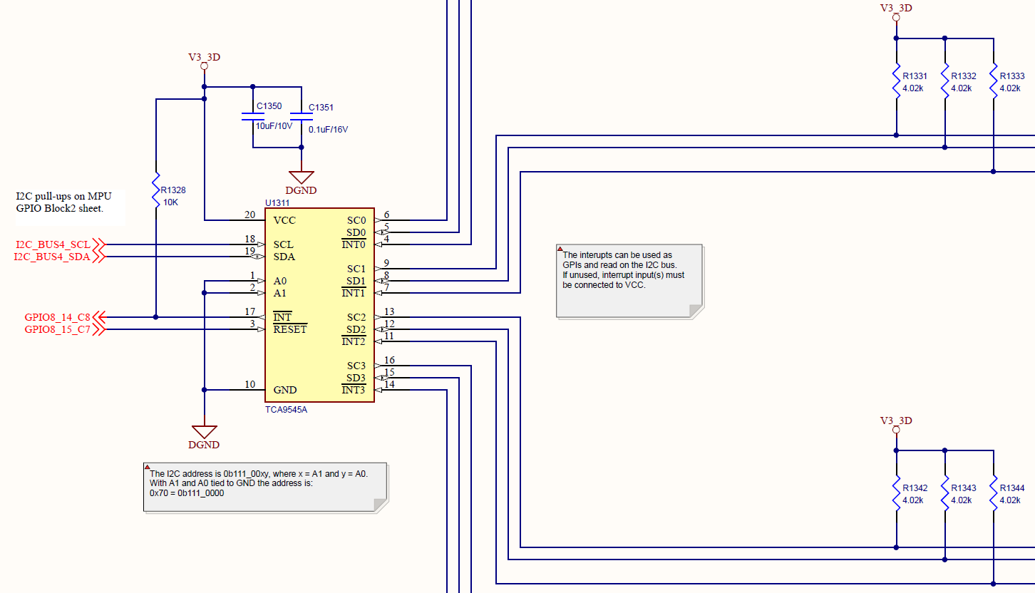
When setting or asking for the active I2C channel the switch responds as expected. However, there is no activity whatsoever on the "channel side" when trying to communicate with devices connected to any of the channels. All channels are stuck at logic high. It's like the pass-gate transistors never turn on and let anything through.

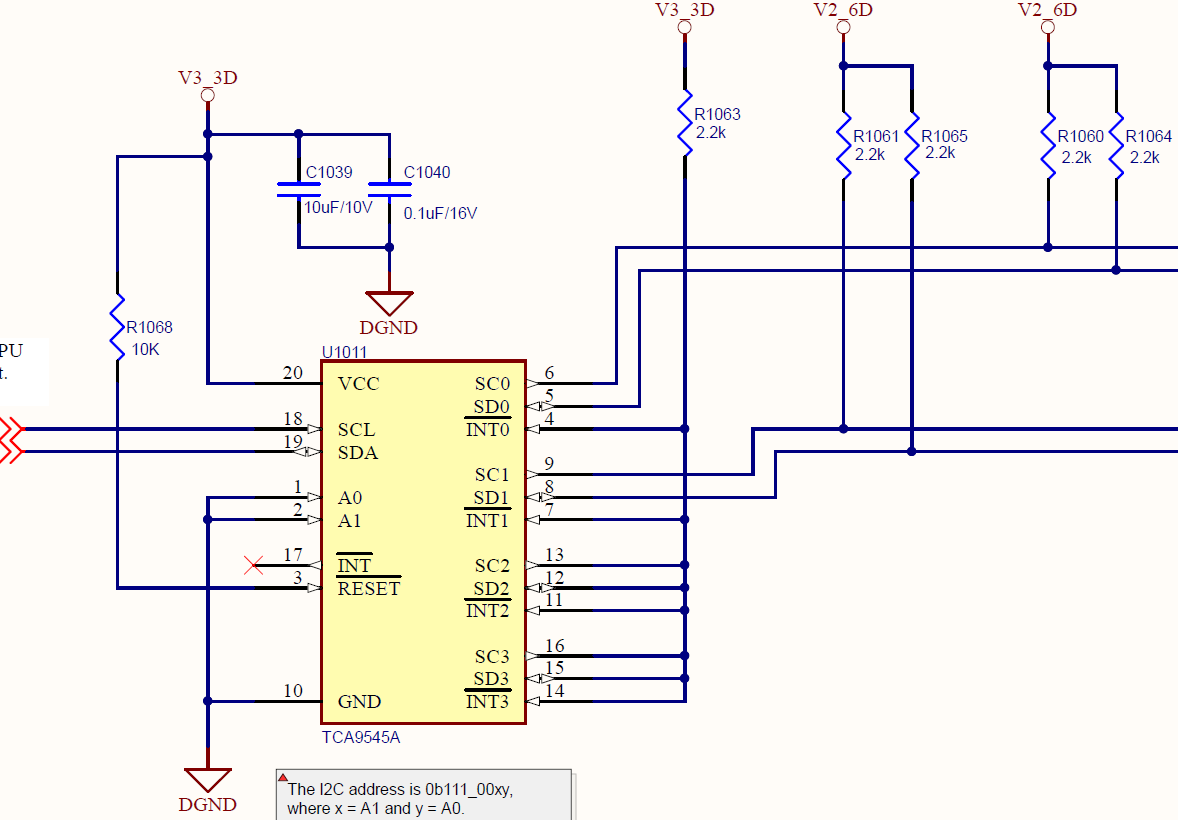
The 2.6 V on the right side should be ok according to the datasheet figure 17 and page 18. I'm not sure about the unused interrupts and unused channels though. Could the pull-up to 3.3 V cause any problems?

Regards

F

  • Hi Fredda,

    The TCA9545A has a control register that is used to determine which channels are active - they are all disabled by default at power up. (See page 15 of the datasheet for details.) Are you writing to this register to enable the channels that you want to use?

    Pulling up unused ports should be OK.

    Regards,
    Max
  • Hi,

    Yes, we are writing to this register to enable the channel we want to activate. We have another TCA9545A on the same board that is working without any problems. Only difference is that the "channel side" have 4.02 k pull-ups to 3.3 V on SDA, SCL and INT. We are also making use of the INT and RESET IOs on this other TCA9545A instance.

    We have also made a manual RESET by simply shorting the RESET pin with a wire to GND, but that didn't make any difference. Could we have damaged the TCA9545A that is not working in some way? Are there any precautions you should be aware of that we my have missed?

    Regards
    F
  • Fredda,

    So the only difference between the SDA/SCL handling on working and non-working units are the channel-side pull-up resistances/voltages? That's strange, since either 4.02 kOhm or 2.2 kOhm should work (at least, neither should result in the buses to be stuck high).

    I'm still a little concerned with the config register, so I had a couple of questions related to that. Are you able to read back the values that you are writing to verify that the write operation took place successfully? (If not, then it would be good to probe the SDA/SCL lines to verify.) And, are you keeping the unused channels disabled? (This is useful to reduce loading on the bus.)

    And yes, it is possible that the device is damaged although there isn't a particular sensitivity that I am aware of. You may want to try swapping your working and non-working units, though, to see if the problem remains with the IC or with the location on the PCB.

    Max
  • Thanks for the reply. No other difference... Yes we are reading back the config register with success. Confirmed both when looking in the I2C master (AM5718) and when probing the bus with a logic analyzer. Unused channels are disabled. Only one channel is enabled at a time.

    It's really not a complicated device/circuit so yes it's strange! We have tested two different boards with the same result. Although not likely, the switch may be damaged on both boards. Perhaps it's an ESD issue since the slave devices on the two channels are connected to the switch by means of a cable. How sensitive is the switch to ESD? Could the pass-gate transistors be damaged so that nothing passes through? Wild guesses here...

    /F
  • It's possible that transients like ESD could occur and damage the chip in such a way that signals do not properly pass across the switching transistors, but for this to happen on two units seems unlikely. (The pins are rated for 4 kV HBM ESD, so I wouldn't consider them especially vulnerable.)

    Do you see any movement at all on the channel sides when there is switching on SDA/SCL? I was wondering if maybe they were getting pulled down but not to a low enough level. This would show up on an oscilloscope but may not show up on something like a logic analyzer.

    Our team member who is most familiar with this device is out of the office today, but I can discuss this further with him once he returns on Tuesday (Monday is a holiday in the US).

    Max
  • I've been probing the channel side with an oscilloscope and it's stuck at 2.6 V. No sign of any movement at all. It's like the pull-ups are zero-ohm resistors... (they aren't!)


  • Here are some oscilloscope images from the master side (pin 18 and 19). The address of the switch is 0x71 (not 0x70 as shown in the schematic).

    The master sends 111 0001 0 (address = 0x71 and it's a write) and the switch responds with an ACK. Then it seems like the slave releases the line before the master starts to send the control register, which causes a short glitch, but that shouldn't matter. The control bits are 0000 0001 which should activate channel 0 on the switch. After that the clock is held low. Don't know exactly what is going on here, but it seems like the switch stretches the clock by some reason.

    Next image, the master reads back the control register.

    The master sends 111 0001 1 (address = 0x71 and it's a read) and the switch responds with an ACK. The switch sends back 0000 0001 to the master, which corresponds to the what the master wrote in the first step. The master replies with a NACK indicating it's done reading the bus. Again. it seems like the switch makes use of clock stretching.

    Last image, the master tries to communicate with a device on channel 0. Address is 101 0000 (0x50). We got a NACK since the channel side is dead and nothing answers. The purple probe is the SCL line on the channel side.

    Regards

    /F

  • Forgot to mention that our other switch on our board is probably dead as well. We had an address conflict, which fooled us in believing that we were communicating with a device on the other side of the switch when we weren't.
  • More information. The other instance of the switch, which showed to be non-functional as well:

    The downstream devices on this switch are four LM96063 fan controllers and the design is to a large degree based on LM63LM64LM96x63EVM. This EVM works without any problems, but it uses the PCA9545A switch instead of the TCA9545A switch. They are supposed to be identical, aren't they? We are actually using the PCA9545A switch on another custom made board where it's also working without any problems. Are there any differences between the two switches that could cause the PCA9545A to work, but not the TCA9545A?

    /F

  • Hey Fredda,

    What I find odd is the o-scopes show the clock line latching low after the ACK. You've pointed out that it looks like it's the TCA9545A clock stretching but to my knowledge this device does not have the capability to do clock stretching as we usually remove the pull down FET on the SCL line of our devices because our devices do not require much time to parse the data they receive. My guess is the master is the one holding the SCL line low if I am correct (will need to check design files). 

    I also notice that the SCL line does go back high after some point when SDA is pulled low again. Because I2C is open drain, there should be no way for a device to ACTIVELY drive a line high, this means one of two things:

    a: If the slave performed clock stretching then it must have released the SCL line and the master took control again

    b: The master had control the entire time and waited sometime before communicating again

    Just checked design files and it looks like our device is incapable of performing clock stretching so it is likely due to the master or another device with the same address as the switch performing clock stretching.........

    I have seen cases (check the edit below) where the master drives the I2C lines low (and keeps them low) and only releases the line high when it needs to send a 1. Our device does not actually enable the switch's channels until it has successfully seen a stop condition so I am wondering is the master is pulling the line low on SCL and causing the device to never see a stop condition thus never actually turning on the channels.

    I would suggest checking the code for the master to confirm if it is clock stretching for some odd reason.

    Thanks,

    -Bobby

    EDIT: I remembered a similar case like this but both lines were held low instead of SCL. This is likely the same issue though.

  • Thanks for the answer. Seems like it may have to do with the absence of a stop condition. The forum thread you linked to says in a post :

    "You need to generate a STOP condition before the channels are actually actuated. A repeated start or just idle won't actually initiate what is loaded in the register space. "

    Should I interpret this like it doesn't matter that we can actually read back the control register with a '1' for the channel we activated. The '1' hasn't taken effect.

    Regards
    /F
  • Hey Fredda,

    "Should I interpret this like it doesn't matter that we can actually read back the control register with a '1' for the channel we activated. The '1' hasn't taken effect."
    - In the thread I linked the user also stated he was able to read back what value he wrote but it didn't look like he properly initiated a stop condition.

    "Should I interpret this like it doesn't matter that we can actually read back the control register with a '1' for the channel we activated. The '1' hasn't taken effect."
    - I believe so but it may also help (and wouldn't hurt) if we put the reset pin on the o-scope and watch it while you communicate with the device. That would be the only other reason I could think of for a working device to malfunction. (If reset goes low for some reason for too long then it could change the internal register to turn off the enabled channels after we write and have read the internal register).

    Thanks,
    -Bobby
  • Thanks! It turned out that we had the exact same issue. We were trying to both write to and read from the switch in the same I2C transaction. The I2C driver locks the bus, by keeping the clock low, between the two operations with a missing stop condition as a result. By only making a write in a transaction, the stop condition appears right after the write, which makes the switch initiate the channels set in the control byte.

    /F