This thread has been locked.
If you have a related question, please click the "Ask a related question" button in the top right corner. The newly created question will be automatically linked to this question.
Hi Expert,
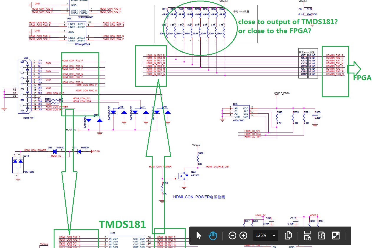
My customer is using the TMDS181 and they are asking a question about the "inductor+resister" network location?
HDMI sink:
HDMI connector => TMDS181 => INDUCTOR + RESISTER NETWORK => FPGA
does INDUCTOR+RESISOTER NETWORK close to the output of TMDS181 or close to the FPGA? why?
Customer's schematic:
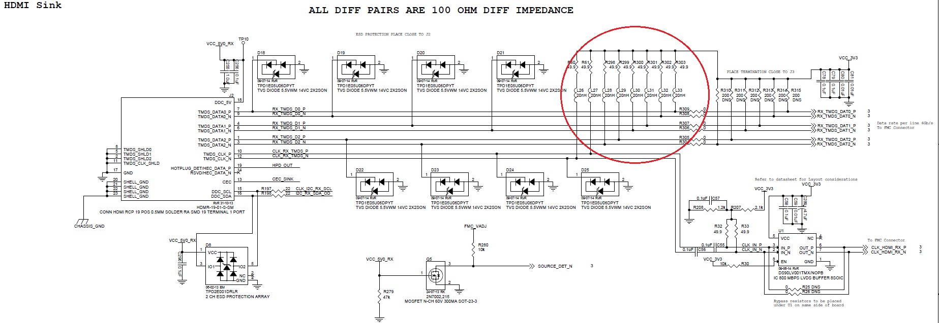
Some HDMI sink reference design from the thrid party:
Best Regards
Iven Xu
Hi Malik,
could you please clarify what's your explanntion? I cannot understand your point.
1, TMDS181 be used as the SINK mode in this application.
2, where do customer need to add this kind of biasing network?
Based on your last sentence: add this kind of RL network between HDMI connector and TMDS181?
Based on your first sentence: need to add the RL network between TMDS181 and AC CAP+ FPGA?
Best Regards
Iven Xu
Iven,
1. This is correct
2. The RL network should be placed between connector and TMDS181.
Notes:
It appears the RL network will cutoff biasing to TMDS181 when there is a high speed signal on the Data lanes. For this reason a 50 ohm pull up to 3.3V should be used between TMDS181 and AC Cap + FPGA. Driver on TMDS181 still needs to be biased correctly when enabled.