This thread has been locked.

If you have a related question, please click the "Ask a related question" button in the top right corner. The newly created question will be automatically linked to this question.

SN6501: How do I reduce back emitted EMI due to SN6501 switching.

Part Number: SN6501
Other Parts Discussed in Thread: SN6505A

Hi,

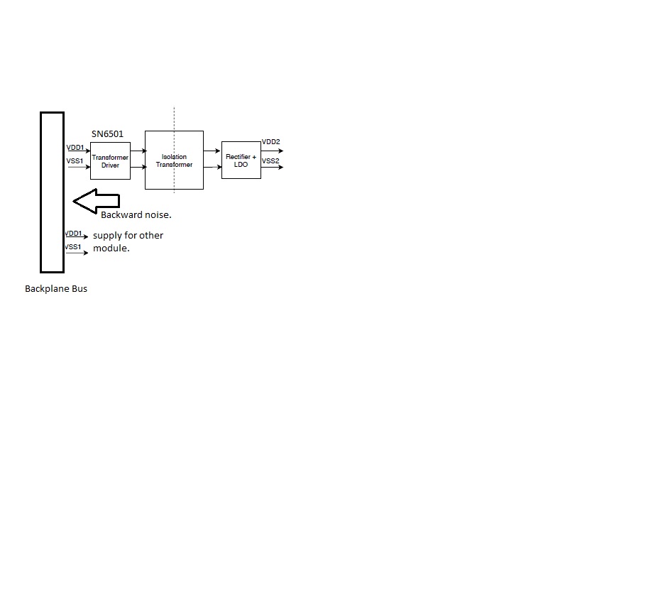
I am using SN6501 for 5V to 5V isolated DC-DC power supply design.

I am using local 5V supply to provide VCC to SN6501. This 5V is output of a separate DC-DC converter. The same local 5V supply is used for other module also.

My question is, When SN6501 operates, due to switching it will throw a conducted EMI noise in this 5V supply lines.

Due to noise on 5V supply the other module may malfunction.

Please suggest solution to this problem.

Regards,

Prasad.

  • Hi Prasad,

    Thanks for using TI E2E forums. We'll try to suggest some solutions for you. Let us say Vcc1 = local 5V supply = output of your DC-DC converter; Vcc2 = isolated 5V output generated by SN6501.

    Option 1:

    The 6501 uses a balanced push-pull topology, which is generally very helpful for a low baseline EMI signature to start-with.  It does have a fixed frequency and rise/fall times, so basically you only have two knobs to further reduce any small kickback voltage ( L *di/dt) generated  during switching. One is to use a transformer with low _leakage_ inductance (the L component) and the other knob is try and reduce the load current (the di component).  On top of this , you can consider using pi filters on the supply lines to target any problem frequencies.

    Option 2:  

    You can consider upgrading to SN6505, which offers additional features, but also provides additional ways to control/reduce EMI.  It comes in two versions, 6505A and 6505B, which differ in the clock frequency of the internal oscillator and you can pick one which suits your needs better, in terms of frequencies of concern in your system.  It also offers slew rate control  and has built-in Spread Spectrum Clocking,  both of which help in lowering EMI peaks.  You also can sync to an external clock for really tight control of system harmonics.

    Debug steps to consider:

    The DC-DC converter used for generating Vcc1 (local 5V supply per above) will also have its own signature. So it's important to understand how much EMI that contributes standalone. for this purpose, I recommend testing the module with a known good lab supply (5V), then testing it with a Vcc1 alone, testing it with Vcc2 alone, and then with everything combined, so you know precisely which component in your system is contributing. It is likely to be a combination of all of the above also.

    Questions:

    1) Could you please let us know if you are you trying to meet any emissions standards, or at this point you are focused on module functionality?

    2) if possible, can you please provide a simplified block diagram of the system ? Always helps for analysis ...

    Thanks,

    Abhi

  • Hello Abhi,

    Thanks for update !

    Our main concern is to stop or reduce conducted EMI which travels backward to our backplane bus.

    VDD1 = local 5V supply

    VSS1 = GND of local 5V supply.

    VDD2 = 5V isolated supply

    VSS2 = Isolated GND

    As per figure, if back noise is present on VDD1 and VSS1 it will travel to next module also via common backplane bus. So the other module may malfunction.

    hence, we want to stop this back noise thrown by SN6501. Please guide.

    Regards,

    Prasad.

  • Hi Prasad,

    Thank you for your patience.
    In this case, I would consider Option #2 in my post above and consider upgrading to SN6505A. It has lower switching frequency and is also slew rate controlled. And it has the spread-spectrum implementation on top of this. All of this will help in further minimizing EMI.
    You can try this out and verify the performance. Size and pinout of 6505 is very similar to SN6501.


    Additional solutions (_optional_):
    1) You could insert a low forward drop Schottky diode in between your backplane bus and the VDD1 power supply to SN6501/6505. This will allow forward power transfer, but will block any reverse injection back to the backplane bus. The tradeoff here is slight efficiency loss = (diode drop) * ( primary current).

    2) You could insert pi filtering between the backplane and the vdd1 supply.

    The 6505 has good performance and these additional options will help you to reduce the EMI signature further.

    Hope this helps!
    Best regards,
    Abhi
  • Hi Prasad,

    I have left this thread open to allow for follow-up questions/responses.
    Please feel free to post additional specifics as desired.

    Thanks,
    Abhi
  • Hi Prasad,

    It's been a while, so just wanted to check if you had any further questions or were able to resolve the issue.

    I would like to close this thread for now, but if help is still needed, you are always welcome to use the buttons at the top right of this page to either "Ask a related question" or "Ask a new question".

    Best regards,
    Abhi