This thread has been locked.

If you have a related question, please click the "Ask a related question" button in the top right corner. The newly created question will be automatically linked to this question.

DP83867CR: Rx clock signal with slow Rise and Fall time

Part Number: DP83867CR

Dear Colleagues and TI team,

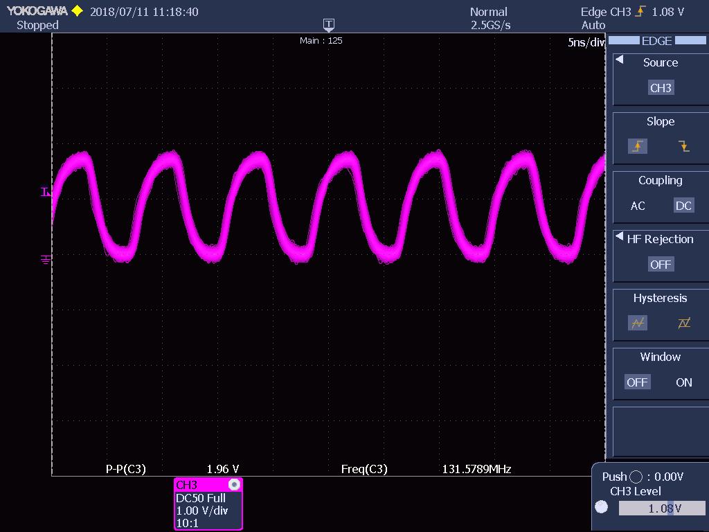
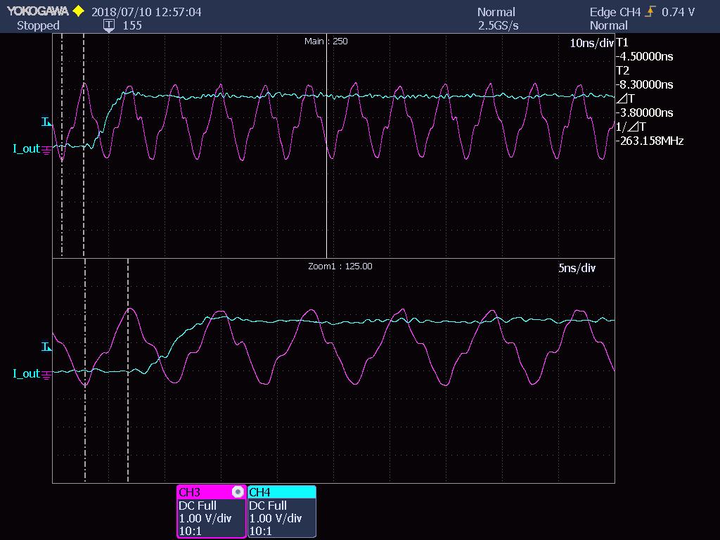
I've developed a board with several DP83867CR PHYs that are connected to the Zynq 7030 on a separated board (manufactured by KnowRes) and I am having troubles getting it to work. After some weeks checking the PHY and the MAC configurations, I measured the RGMII signals with a fast scope (BW of 1GHz) and an active FET probe. For my surprise, the rx_clk is as you can see in the figure below. The rise and fall times (~4ns) are several times more than the values stated in the datasheet (<0.75ns).

I checked the PHY power supply and clock out pin and they seem to be fine. The PHY is connected directly (no damping resistors added) using 50 ohm traces to the connector. Which could be the reason for such clock signal?

Enclosed is the an extract of the board schematics.

2352.sch.pdf

KR,

Tomas

  • Hi Tomas,

    You should see a square wave and not a sine wave.
    How long are the traces?
    What is the loading at the Zynq?
    Does each signal line have solid ground beneath it?
    Any layout images you can share?
  • Hi, Ross,

    The traces are ~1560 mil long at the carrier board + a bit more at the module board. 

    The Zynq maximum die capacitance is 8 pF according to the datasheet (not including package capacitance). The probe has 1.8pF.

    Signals tracks are in Top and Bottom layers; Layers 2 and 5 are ground plane layers.

    Below you can see a part of the pcb board (I could share a pdf or the altium or the gerber files, if you prefer). The signal highlighted is the rx_clk:

    And the layer stack-up:

    Please advise if I you need any additional info. Thanks for the help!

    Tomas

  • Hi,

    some additional information regarding this problem. I measured the tx_clk signal and the waveform is similar:

    TX_CLK                                                                                                      RX_CLK


    Then I removed the Zynq board and measured the Rx_clk (of course, there was no Tx_clk to be measured):

    rx_clk

    So, this is the kind of waveform I would expect to see. Next, I changed the TX_CLK pin strength and slew rate in the Zynq and got this waveform:

    tx_clk

    I searched to similar settings for the DP83867, but I could not really find. It seems that the PHY driver is too weak to the line, but its not really a long line with so much load. What do you think? Is there any other possibility or possible reason that the PHY driver does not have enough current to produce a square wave?

    KR,

    Tomas

  • Hi Tomas,

    RGMII spec is for a max 5pF load. You might need to place a redriver in the path to reduce the rise/fall time.
    We do not have a register for increasing the drive strength of the IO.
  • Hi, Ross,

    I see. Would increasing the VDDIO voltage (from 1.8V to 2.5)  improve it a bit or you think that the external drive is my only chance?

    Regards,

    Tomas

  • I would think so.
    There is not much drive strength with a 1.8V IO.
    The VOH/VOL numbers for a 1.8V IO are spec at 1mA load while 2.5V IO at 4mA.
    That extra 3mA might give you the needed boost.