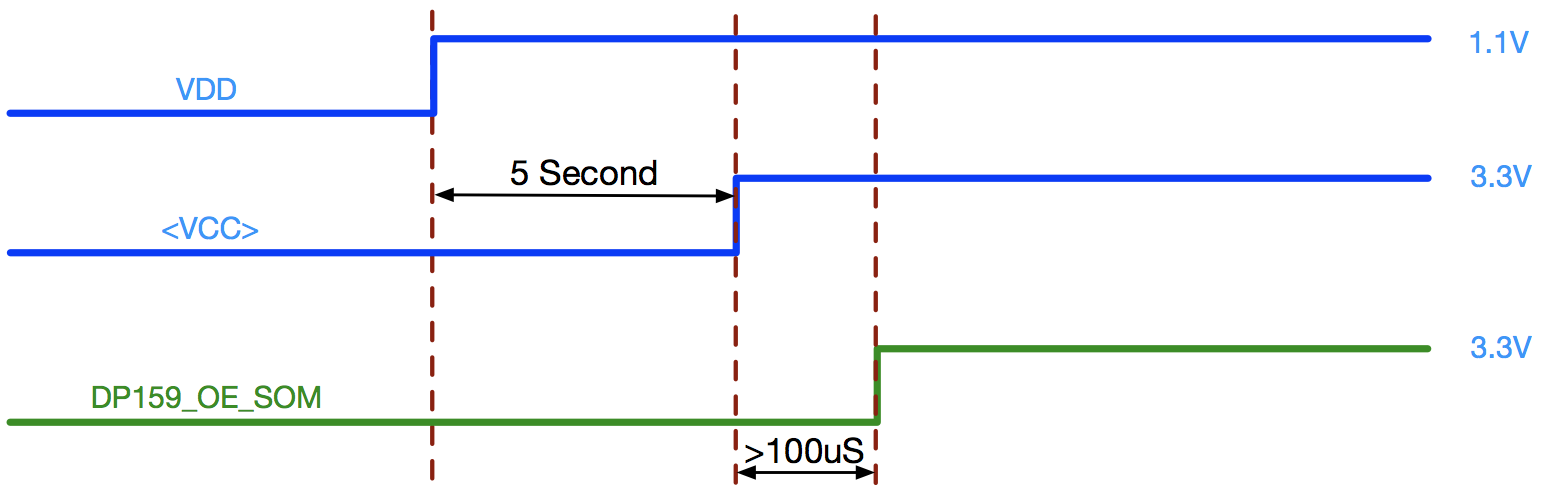
Hi, I attached the captures of power on timing section of DP159.
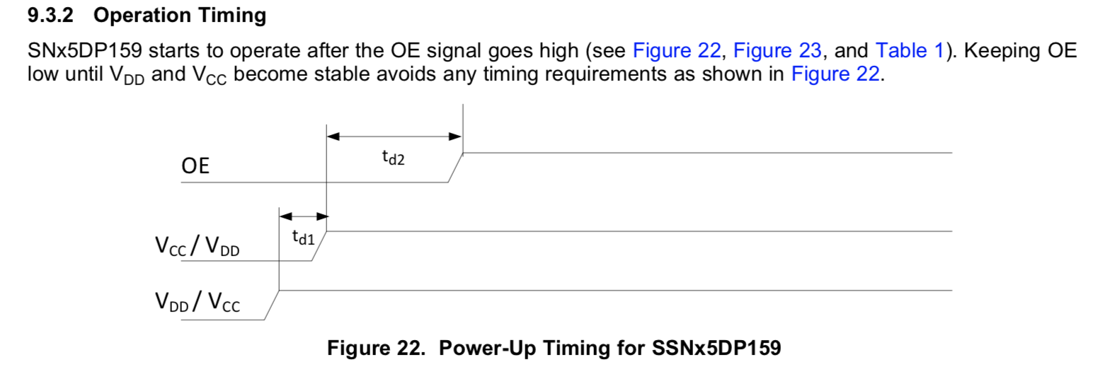
Figure 22 is confusing to me: why there is VCC/VDD, and VDD/VCC? How to understand td1? Is there a specific timing requirement of VCC and VDD on which should ramp first?
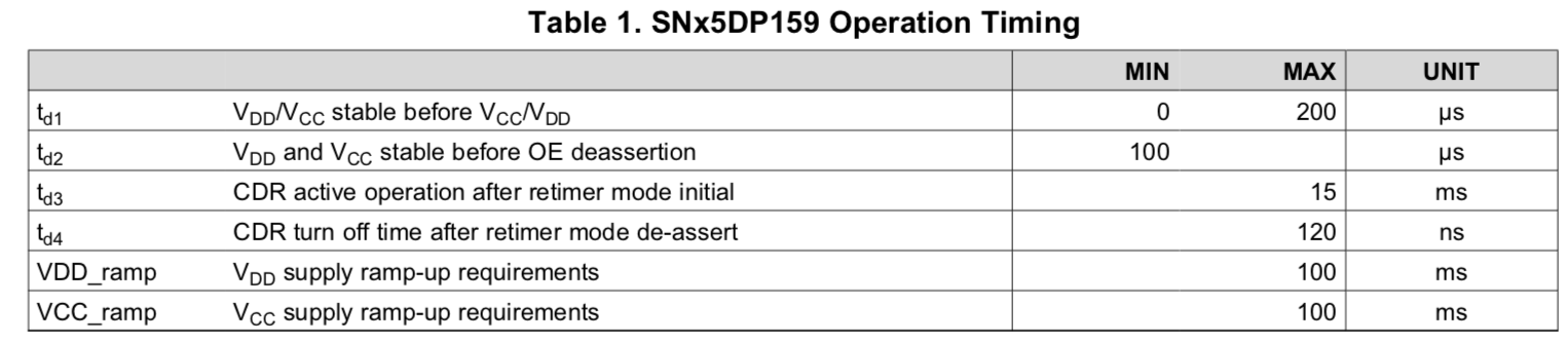
td1 is specified at max = 200us. If I apply VCC first, then VDD must start ramping within 200us?
From this thread, there is no requirement of sequence VCC, VDD as long as OE is LOW.
Thank you.