Part Number: SN75DP159
We are failing FCC Class B EMC testing by a huge margin, and are looking for any additional ideas regarding the possible cause (see example frequency scan below; one channel active).
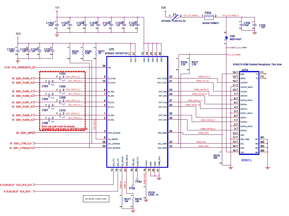
We are using two SN75DP159 devices driven by two DDI outputs from a COM Express module, to HDMI. A representative schematic is show below for one channel.
Layout summary:
- We have tight intra (5mil) and inter (20mil) lenght matching of DDI and HDMI traces
- Good trace impedance control: 100 ohm differential
- DDI trace lengths are about 3.5 inches from COM Express to SN75DP159; 2 vias each trace; uninterrupted GND plane above and below; same layers used for all traces
- HDMI trace lengths ar about 6.5 inches from SN75DP159 to HDMI connector; 2 vias each trace; uniterrupted GND plane above and below; same layers used for all traces
- ESD protection devices located right at HDMI connector
We have tried reducing the slew rate and voltage swing of data and clock, and added de-emphasis, but these had no impact on measured far-field EMI.
Our test setup:
Two 25 foot HDMI cables (seem well constructed and shielded)
Two displays located OUTSIDE of test chamber
It seems we are missing something major to be failing to such an extreme degree.