This thread has been locked.

If you have a related question, please click the "Ask a related question" button in the top right corner. The newly created question will be automatically linked to this question.

PCA9306: About Max output voltage and Min output voltage

Part Number: PCA9306

Hi,

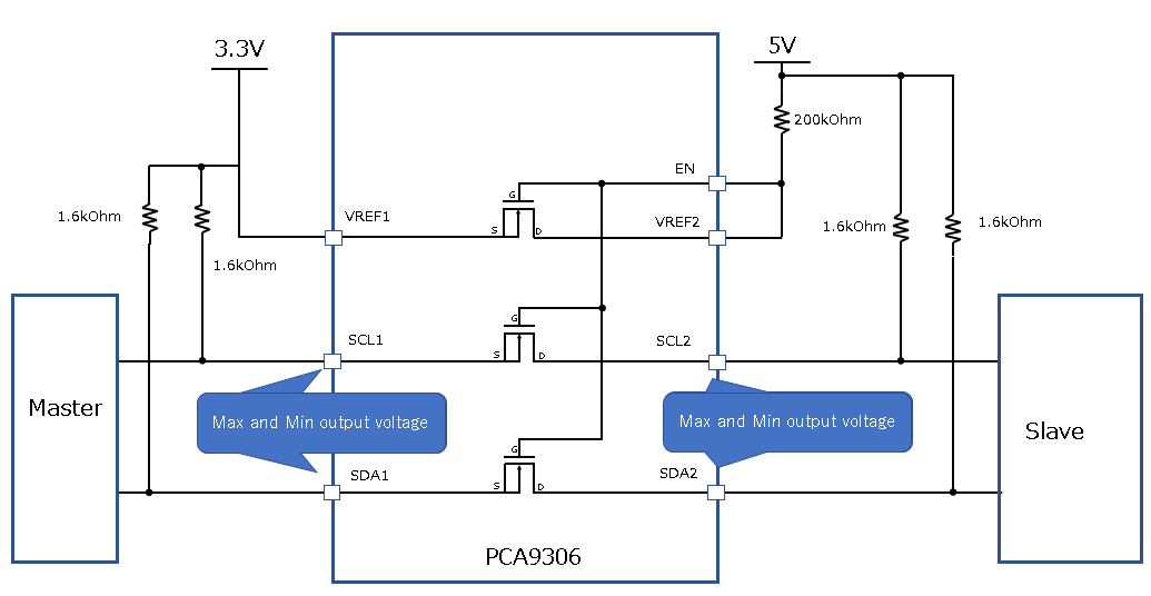
I think of using PCA9306 below circuit.
But Max output voltage and Min aren't defined in datasheet.
Could you let me know Max output voltage and Min output voltage of SCL1/2 and SDA1/2, please?
and could you let me know formula for caluculating this, please?

Best regards,
Shimizu

  • Hello Shimizu-san,

    This device works by providing a low-impedance connection between sides 1 and 2 (i.e., pass FET turned "on") when a low voltage is present on either side and by staying high-impedance otherwise. This means that the maximum voltage on the SDA/SCL lines would be equal to the pull-up voltages used. The minimum SDA/SCL voltages would be equal to the output low level of the I2C master or slave device that is pulling the line low.

    I hope this info is helpful - please let me know if it is unclear or if you have further questions.

    Regards,
    Max
  • Hi Max,

    Thank you for your support.
    If nobody drive to low, Is internal switch disable?
    For the reason, The side of 1 and 2 is pulled up by REF?

    Best regards,
    Shimizu

  • Shimizu-san,

    Yes, this is correct. If neither side is driven low, the internal switch is disabled (high impedance), allowing each side to be pulled up to its own pull-up reference voltage.

    Max
  • Hi Max,

    Thank you for your reply.
    I add a question.

    Could you let me know threshold voltage level of input signal voltage to change of internal switch status, please?

    Condition is the circuit of above post.

    Especially, I want to know about signal level from slave(VREF2 side).
    From how voltage is internal switch to be ON? => Vil
    From how voltage is internal switch to be OFF? => Vih

    Best regards,
    Shimizu

  • Shimizu-san,

    The device will internally regulate the bias voltage on the pass-FET gates to be one threshold voltage greater than VREF1 (assuming that VREF2 is at least 600 mV greater than VREF1). So, as the voltage on either side decreases below the VREF1 level the switch will start to conduct.

    Regards,
    Max