This thread has been locked.

If you have a related question, please click the "Ask a related question" button in the top right corner. The newly created question will be automatically linked to this question.

DS90UB954-Q1: DS90UB954-Q1 CSI-2 output has good data but no clock.

Part Number: DS90UB954-Q1

I have a DS90UB954-Q1 down on my board.  It is receiving two streams on its' two RX ports.  The two streams are synchronized and the 954 is using its' "Line-Interleaved Forwarding" engine to output the data on 4 lanes of its' CSI-2 bus.  Everything looks pretty good on the scope except I have no CSI-2 clock.  I have been all through the register settings (especially the 0x33 - 0x38 regs) and I cannot find a problem with them.  I am setup for continuous clocking.  Does anyone have any ideas on what may be happening here?

  • I have checked all the pin and the boot up sequencing and everything seems correct. I inherited a lot of the initial code running in a separate micro which sets up the 954 and the attached (via coax) 953's. Also, there is a lot of code in the beginning which seems to relate to earlier silicon. Some of it I have not idea what it is doing.. I am listing it here so if you know that this code is not needed or could be a problem for my setup let me know. I am only including the initialization code that is at the top of Main which is using a bunch of the indirect register writes.. Also, where can I get a look at these registers?

    Once more, everything seems to be working from the 953's sending down two sync'd streams and the 954 is able to put them back together and output them as a single stream from the CSI-2 transmitter. My problem is that the transmitter is not putting out a clock.

    thanks,
    david


    I2C_Buffer[0] = 0xB0;
    I2C_Buffer[1] = 0x1C;
    if (HAL_I2C_Master_Transmit(&hi2c1, (uint16_t)DS954, I2C_Buffer, 2, I2C_Timeout) !=HAL_OK)
    printf("I2C transmit error\r\n");

    I2C_Buffer[0] = 0xB1;
    I2C_Buffer[1] = 0x15;
    if (HAL_I2C_Master_Transmit(&hi2c1, (uint16_t)DS954, I2C_Buffer, 2, I2C_Timeout) !=HAL_OK)
    printf("I2C transmit error\r\n");

    I2C_Buffer[0] = 0xB2;
    I2C_Buffer[1] = 0x30;
    if (HAL_I2C_Master_Transmit(&hi2c1, (uint16_t)DS954, I2C_Buffer, 2, I2C_Timeout) !=HAL_OK)
    printf("I2C transmit error\r\n");

    HAL_Delay(100);

    // SBPLL CSI Charge-LOW
    printf("SBPLL CSI Charge-Low, 3 writes\r\n");

    I2C_Buffer[0] = 0xB0;
    I2C_Buffer[1] = 0x1C;
    if (HAL_I2C_Master_Transmit(&hi2c1, (uint16_t)DS954, I2C_Buffer, 2, I2C_Timeout) !=HAL_OK)
    printf("I2C transmit error\r\n");

    HAL_Delay(100);

    I2C_Buffer[0] = 0xB1;
    I2C_Buffer[1] = 0x15;
    if (HAL_I2C_Master_Transmit(&hi2c1, (uint16_t)DS954, I2C_Buffer, 2, I2C_Timeout) !=HAL_OK)
    printf("I2C transmit error\r\n");

    HAL_Delay(100);

    I2C_Buffer[0] = 0xB2;
    I2C_Buffer[1] = 0x30;
    if (HAL_I2C_Master_Transmit(&hi2c1, (uint16_t)DS954, I2C_Buffer, 2, I2C_Timeout) !=HAL_OK)
    printf("I2C transmit error\r\n");

    HAL_Delay(100);


    // P954__SETUP_A0_4G.py
    printf("P954__SETUP_A0_4G.py\r\n");

    printf("Select Ports 0 & 1\r\n");
    I2C_Buffer[0] = 0x4c;
    I2C_Buffer[1] = 0x03;
    if (HAL_I2C_Master_Transmit(&hi2c1, (uint16_t)DS954, I2C_Buffer, 2, I2C_Timeout) !=HAL_OK)
    printf("I2C transmit error\r\n");

    HAL_Delay(100);

    printf("DISABLE LINK PARITY ERROR\r\n");
    I2C_Buffer[0] = 0xB6;
    I2C_Buffer[1] = 0x18;
    if (HAL_I2C_Master_Transmit(&hi2c1, (uint16_t)DS954, I2C_Buffer, 2, I2C_Timeout) !=HAL_OK)
    printf("I2C transmit error\r\n");

    HAL_Delay(100);

    printf("DISABLE DCA CRC\r\n");
    I2C_Buffer[0] = 0xBA;
    I2C_Buffer[1] = 0x83;
    if (HAL_I2C_Master_Transmit(&hi2c1, (uint16_t)DS954, I2C_Buffer, 2, I2C_Timeout) !=HAL_OK)
    printf("I2C transmit error\r\n");

    HAL_Delay(100);


    printf("TF Control Settings, 5 writes, channel 0\r\n");
    I2C_Buffer[0] = 0xB0;
    I2C_Buffer[1] = 0x04;
    if (HAL_I2C_Master_Transmit(&hi2c1, (uint16_t)DS954, I2C_Buffer, 2, I2C_Timeout) !=HAL_OK)
    printf("I2C transmit error\r\n");

    HAL_Delay(100);

    I2C_Buffer[0] = 0xB1;
    I2C_Buffer[1] = 0x04;
    if (HAL_I2C_Master_Transmit(&hi2c1, (uint16_t)DS954, I2C_Buffer, 2, I2C_Timeout) !=HAL_OK)
    printf("I2C transmit error\r\n");

    HAL_Delay(100);

    I2C_Buffer[0] = 0xB2;
    I2C_Buffer[1] = 0x3F;
    if (HAL_I2C_Master_Transmit(&hi2c1, (uint16_t)DS954, I2C_Buffer, 2, I2C_Timeout) !=HAL_OK)
    printf("I2C transmit error\r\n");

    HAL_Delay(100);

    I2C_Buffer[0] = 0xB1;
    I2C_Buffer[1] = 0x14;
    if (HAL_I2C_Master_Transmit(&hi2c1, (uint16_t)DS954, I2C_Buffer, 2, I2C_Timeout) !=HAL_OK)
    printf("I2C transmit error\r\n");

    HAL_Delay(100);

    I2C_Buffer[0] = 0xB2;
    I2C_Buffer[1] = 0x3F;
    if (HAL_I2C_Master_Transmit(&hi2c1, (uint16_t)DS954, I2C_Buffer, 2, I2C_Timeout) !=HAL_OK)
    printf("I2C transmit error\r\n");

    HAL_Delay(100);


    printf("TF Control Settings, 5 writes, channel 1\r\n");
    I2C_Buffer[0] = 0xB0;
    I2C_Buffer[1] = 0x08;
    if (HAL_I2C_Master_Transmit(&hi2c1, (uint16_t)DS954, I2C_Buffer, 2, I2C_Timeout) !=HAL_OK)
    printf("I2C transmit error\r\n");

    HAL_Delay(100);

    I2C_Buffer[0] = 0xB1;
    I2C_Buffer[1] = 0x04;
    if (HAL_I2C_Master_Transmit(&hi2c1, (uint16_t)DS954, I2C_Buffer, 2, I2C_Timeout) !=HAL_OK)
    printf("I2C transmit error\r\n");

    HAL_Delay(100);

    I2C_Buffer[0] = 0xB2;
    I2C_Buffer[1] = 0x3F;
    if (HAL_I2C_Master_Transmit(&hi2c1, (uint16_t)DS954, I2C_Buffer, 2, I2C_Timeout) !=HAL_OK)
    printf("I2C transmit error\r\n");

    HAL_Delay(100);

    I2C_Buffer[0] = 0xB1;
    I2C_Buffer[1] = 0x14;
    if (HAL_I2C_Master_Transmit(&hi2c1, (uint16_t)DS954, I2C_Buffer, 2, I2C_Timeout) !=HAL_OK)
    printf("I2C transmit error\r\n");

    HAL_Delay(100);

    I2C_Buffer[0] = 0xB2;
    I2C_Buffer[1] = 0x3F;
    if (HAL_I2C_Master_Transmit(&hi2c1, (uint16_t)DS954, I2C_Buffer, 2, I2C_Timeout) !=HAL_OK)
    printf("I2C transmit error\r\n");


    HAL_Delay(100);

    printf("Adjust EQ Default Settings, 7 writes, channel 0\r\n");
    I2C_Buffer[0] = 0xB0;
    I2C_Buffer[1] = 0x04;
    if (HAL_I2C_Master_Transmit(&hi2c1, (uint16_t)DS954, I2C_Buffer, 2, I2C_Timeout) !=HAL_OK)
    printf("I2C transmit error\r\n");

    HAL_Delay(100);

    I2C_Buffer[0] = 0xB1;
    I2C_Buffer[1] = 0x0E;
    if (HAL_I2C_Master_Transmit(&hi2c1, (uint16_t)DS954, I2C_Buffer, 2, I2C_Timeout) !=HAL_OK)
    printf("I2C transmit error\r\n");

    HAL_Delay(100);

    I2C_Buffer[0] = 0xB2;
    I2C_Buffer[1] = 0x20;
    if (HAL_I2C_Master_Transmit(&hi2c1, (uint16_t)DS954, I2C_Buffer, 2, I2C_Timeout) !=HAL_OK)
    printf("I2C transmit error\r\n");

    HAL_Delay(100);

    printf("Adjust EQ Default Settings, 7 writes, channel 1\r\n");
    I2C_Buffer[0] = 0xB0;
    I2C_Buffer[1] = 0x08;
    if (HAL_I2C_Master_Transmit(&hi2c1, (uint16_t)DS954, I2C_Buffer, 2, I2C_Timeout) !=HAL_OK)
    printf("I2C transmit error\r\n");

    HAL_Delay(100);

    I2C_Buffer[0] = 0xB1;
    I2C_Buffer[1] = 0x0E;
    if (HAL_I2C_Master_Transmit(&hi2c1, (uint16_t)DS954, I2C_Buffer, 2, I2C_Timeout) !=HAL_OK)
    printf("I2C transmit error\r\n");

    HAL_Delay(100);

    I2C_Buffer[0] = 0xB2;
    I2C_Buffer[1] = 0x20;
    if (HAL_I2C_Master_Transmit(&hi2c1, (uint16_t)DS954, I2C_Buffer, 2, I2C_Timeout) !=HAL_OK)
    printf("I2C transmit error\r\n");
  • Hi,
    To be simple, can you check whether UB954 has CSI2 clock output when it is set as pattern generation mode? thanks.

    best regards,
    Steven
  • Hello Steven,

    No CSI-2 clock is coming out, but I do see the data.

    thanks,

    david

  • Hello Steven,

    I did the Test Pattern Generator test...  --> No CSI-2 clock is coming out with TPG.  I do see data with the TPG and with my sourcing it via the two 953's but neither has a clock.

    Also, I have been changing various 954 registers to see if I could get a clock but have not been able to get one.  In one experiment I changed register 0x33 from 0x03 to 0x01 which should cause the clock to stop during the LP portion of the waveform.  When I did this I did see the clock line go high during the LP portion of the waveform (as it should) but there still was no clock on the HS portion of the waveform.  At a minimum this shows that the pins are not be influenced by the pcb or the bad soldering.  Also, I have the same thing happening on two different boards.

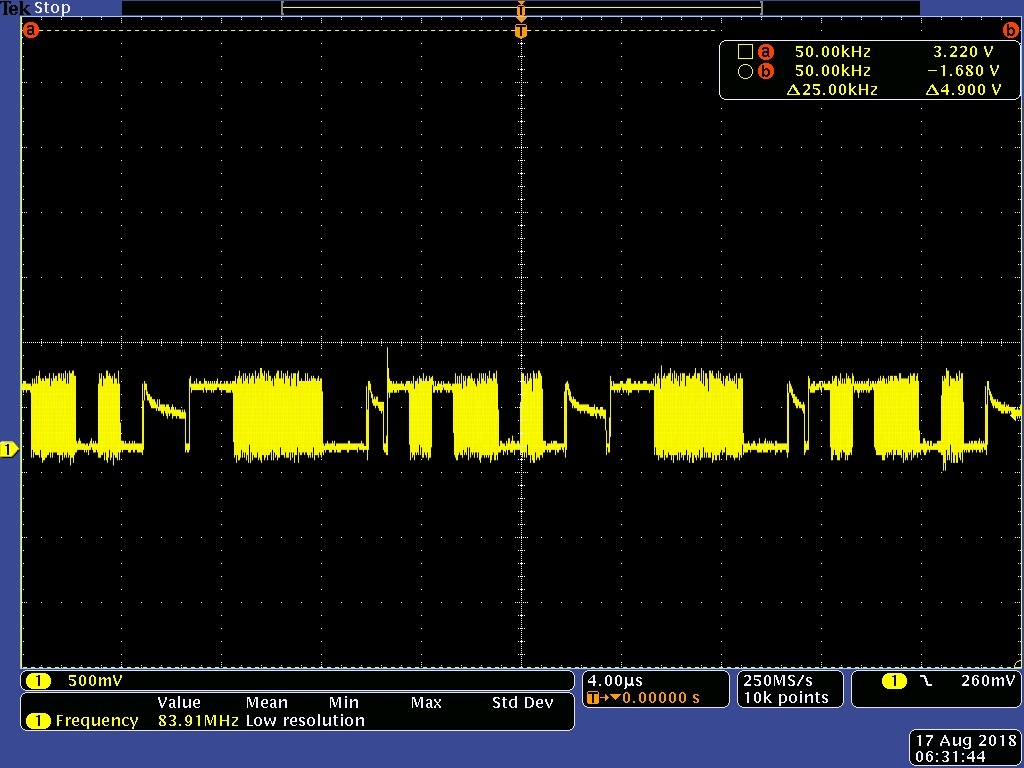
    Also, previously the LP sections of the data signals had looked very strange as shown right below.

    You can see that they look like they are not being terminated correctly but through my experimentation with the registers I was able to fix this.  I simply removed a write to register 0x34.  I had been setting it up to do periodic skew adjust after the frame sync with a write of 0x01.  I simply took that out and the waveform now looks like the following:

    So, it looks like something internal to the part is not allowing the clock to get to the CSI-2 pins...  but the level shifting part of the logic does get there as shown by the level change when I took it out of "continuous clock mode". 

    How is the clock sourced to the CSI-2 clock outputs?

    thanks,

    david

  • Again, what are those indirect register writes doing that I listed above? I see a bunch of them in an earlier users guide having to do with fixes for early silicon eratta. I am concerned maybe some of them are at the root of this problem

    david
  • Hi David,

    It is possible that your CSI_CLK is not enabled. They can be enabled by setting register 0x34:

    Reg 0x34 Reg Name: CSI_CTL2  Bits Field   Type  Default Value  Description
        7 CSI_CLK1_EN RW 0 Enable CSI_CLK1 output
    When this bit is set, the CSI_CLK1 will output the CSI clock signal.  Note, the CSI_CLK1 output will also be enabled if the CSI_REPLICATE control is set in the FWD_CTL2 register.
        6 CSI_CLK0_EN RW 1 Enable CSI_CLK0 output
    When this bit is set, the CSI_CLK0 will output the CSI clock signal.  Note, the CSI_CLK0 output will also be enabled if the CSI_REPLICATE control is set in the FWD_CTL2 register.
        5:4 RESERVED R 0x0 Reserved
        3 CSI_PASS_MODE RW 0 CSI PASS indication mode
    Determines whether the CSI Pass indication is for a single port or all enabled ports.
    0 : Assert PASS if at least one enabled Receive port is providing valid video data
    1 : Assert PASS only if ALL enabled Receive ports are providing valid video data
        2 CSI_CAL_INV RW 0 CSI Calibration Inverted Data pattern
    During the CSI skew-calibration pattern, the CSI Transmitter will send a sequence of 01010101 data (first bit 0).  Setting this bit to a 1 will invert the sequence to 10101010 data.
        1 CSI_CAL_SINGLE RW/SC 0 Enable single periodic CSI Skew-Calibration sequence
    Setting this bit will send a single skew-calibration sequence from the CSI Transmitter.  The skew-calibration sequence will be the 1010 bit sequence required for periodic calibration.  The calibration sequence will be sent at the next idle period on the CSI interface.  This bit is self-clearing and will reset to 0 after the calibration sequence is sent.
        0 CSI_CAL_PERIODIC RW 0 Enable periodic CSI Skew-Calibration sequence
    When the periodic skew-calibration sequence is enabled, the CSI Transmitter will send the periodic skew-calibration sequence following the sending of Frame End packets.
    0: Disabled
    1: Enabled

    Right now the upper four bits from reg 0x34 are showing as reserved. Fixes will be made in the upcoming datasheet revision.

    Best,

    Jiashow

  • Hi Jiashow,

    I'm at home right now but this may be it.  I want to say that my register 0x34 is 0x00.  I believe I remember that was the default and this is the register that I commented out to fix the waveform shapes.  Do you have an updated registers listing that I can get.  I'm pretty sure that my data sheet does not have this information for register 0x34.

    thanks,

    david

  • Hi David,

    All other relevant register descriptions are included in the datasheet. We will be including the updated register 0x34 description in the next revision.

    Best,
    Jiashow
  • Hello Jiashow,

    I had high hopes for the upper bits of register 0x34 but it made no difference.  Still no clock coming out of my CSI-2 port. I also tried various other register values for register 0x34 with no luck.

    One other comment...  Please be aware that I am running a 26Mhz external clock and have CSI_PLL_CTL[1:0] set to 00.  I expect this to give me a CSI-2 TX Frequency of 1664Mbps.  Do you think this could be the issue?  I have a 24Mhz oscillator and I am going to put it on and see if it makes a difference.

    This is a post edit..  I did the change to the 24Mhz external clock and it made no difference.  I am purely running the internal test pattern generator and have completely disconnected the coax lines and taken out the register writes having to do with setting the clock and comms with the 953s...

    Also, I completely removed the external oscillator and tried to run with the internal 25Mhz oscillator first..  That did not help at all..

    It is looking to me like this is not a clock speed issue or having to do with overclocking something internally but rather has to do with the internal clock path being correctly switched to the CSI-2 Clock output..

    david

  • Hello again Jiashow & Leo,

    Here is some more data to try to help solve this... We had a completely seperate platform that we did prior to my current board. It consisted of separate 953 boards and 954 boards. The main difference was that the 954 CSI-2 outputs fed a connector rather than a FPGA. We "thought" we had these boards working, meaning that that we have data showing in the 953 registers and the same line lengths and data arriving in the 954 registers. We also had good lock and ability to output sync'd interleaved data from the 954.

    I had thought that this platform was completely working but I just built it back up and it has the exact same problem. No clock coming out of the CSI-2 output.

    One other comment... talking about my current board again.. I removed all of the indirect writes and various other setups for the larger system. I now only have writes in for setting up register 0x33 with 0x01 and the test pattern generator. I still get the test pattern out of the 954 but no clock. I am running an external 24Mhz clock in this setup.

    I believe that my reset and initialization is correct but I'll scope it and post a pic so you can concur or not.

    david
  • Hi David,

    Could you provide the script you ran to get CSI output from pattern generator? Have you checked CSI continuous clock mode? Some processors need them to be disabled to work.

    Best,

    Jiashow

  • Hi Jiashow,

    The following register dump is from my greatly modified code... Basically all it has in it is the following:
    write to 0x33 = 0x01
    write to 0x34 = 0x41
    all the writes for test pattern example from page 63 of SNLS570 - August 2017

    Note: I am using an external 24Mhz oscillator.

    What I observe with scope:
    I see the test pattern signals on all 4 data pairs (with their LP and HS sections).
    I see the LP and HS transitions on the CLK0 but no actual clock.
    Nothing on CLK1 (as expected).

    I can easily get back to my full code set which I will do. I will post a s second dump from the 954 ports and both 953's.

    Set port selected to port 0
    Registers for Deserializer
    0x00: 0x60, 0x00, 0x1E, 0x20, 0xD3, 0x01, 0x00, 0xFE, 0x1C, 0x10, 0x7A, 0x7A, 0xBF, 0x09, 0x1B, 0x7F,
    0x10: 0x00, 0x00, 0x00, 0x00, 0x00, 0x00, 0x00, 0x00, 0x00, 0x00, 0x00, 0x00, 0x00, 0x00, 0x04, 0x02,
    0x20: 0x30, 0x01, 0x00, 0x00, 0x00, 0x00, 0x00, 0x00, 0x00, 0x00, 0x00, 0x00, 0x00, 0x00, 0x00, 0x00,
    0x30: 0x00, 0x00, 0x00, 0x01, 0x41, 0x00, 0x00, 0x00, 0x00, 0x00, 0x00, 0x01, 0x14, 0x6F, 0x00, 0x40,
    0x40: 0x00, 0xA7, 0x71, 0x01, 0x00, 0x00, 0x00, 0x00, 0x00, 0x00, 0x00, 0x12, 0x01, 0x00, 0x02, 0x00,
    0x50: 0x00, 0x00, 0x00, 0x00, 0x00, 0x00, 0x00, 0x00, 0x1E, 0x00, 0x00, 0x00, 0x00, 0x00, 0x00, 0x00,
    0x60: 0x00, 0x00, 0x00, 0x00, 0x00, 0x00, 0x00, 0x00, 0x00, 0x00, 0x00, 0x00, 0x00, 0x7C, 0x88, 0x88,
    0x70: 0x2B, 0x2C, 0xE4, 0x00, 0x00, 0x00, 0x00, 0xC5, 0x00, 0x01, 0x00, 0x00, 0x20, 0x00, 0x00, 0x00,
    0x80: 0x00, 0x00, 0x00, 0x00, 0x00, 0x00, 0x00, 0x00, 0x00, 0x00, 0x00, 0x00, 0x00, 0x00, 0x00, 0x00,
    0x90: 0x00, 0x00, 0x00, 0x00, 0x00, 0x00, 0x00, 0x00, 0x00, 0x00, 0x00, 0x00, 0x00, 0x00, 0x00, 0x00,
    0xA0: 0x02, 0x0F, 0x00, 0x00, 0x08, 0x18, 0x00, 0x00, 0x00, 0x00, 0x00, 0x00, 0x00, 0x00, 0x00, 0x00,
    0xB0: 0x00, 0x0F, 0x0A, 0x08, 0x25, 0x00, 0x18, 0x00, 0x8C, 0x33, 0x83, 0x74, 0x80, 0x00, 0x00, 0x00,
    0xC0: 0x00, 0x00, 0x00, 0x00, 0x00, 0x00, 0x00, 0x00, 0x00, 0x00, 0x00, 0x00, 0x00, 0x00, 0x00, 0x00,
    0xD0: 0x00, 0x43, 0x94, 0x04, 0x60, 0xF2, 0x00, 0x03, 0x00, 0x00, 0x00, 0x00, 0x00, 0x00, 0x00, 0x00,
    0xE0: 0x00, 0x00, 0x00, 0x00, 0x00, 0x00, 0x00, 0x00, 0x00, 0x00, 0x00, 0x00, 0x00, 0x00, 0x00, 0x00,
    0xF0: 0x5F, 0x55, 0x42, 0x39, 0x35, 0x34, 0x00, 0x00, 0x00, 0x00, 0x00, 0x00, 0x00, 0x00, 0x00, 0x00,

    Set port selected to port 1
    Registers for Deserializer
    0x00: 0x60, 0x00, 0x1E, 0x20, 0xD3, 0x01, 0x00, 0xFE, 0x1C, 0x10, 0x7A, 0x7A, 0xBF, 0x09, 0x1B, 0x7F,
    0x10: 0x00, 0x00, 0x00, 0x00, 0x00, 0x00, 0x00, 0x00, 0x00, 0x00, 0x00, 0x00, 0x00, 0x00, 0x04, 0x02,
    0x20: 0x30, 0x01, 0x00, 0x00, 0x00, 0x00, 0x00, 0x00, 0x00, 0x00, 0x00, 0x00, 0x00, 0x00, 0x00, 0x00,
    0x30: 0x00, 0x00, 0x00, 0x01, 0x41, 0x00, 0x00, 0x00, 0x00, 0x00, 0x00, 0x01, 0x14, 0x6F, 0x00, 0x40,
    0x40: 0x00, 0xA7, 0x71, 0x01, 0x00, 0x00, 0x00, 0x00, 0x00, 0x00, 0x00, 0x12, 0x12, 0x40, 0x02, 0x00,
    0x50: 0x00, 0x00, 0x00, 0x00, 0x00, 0x00, 0x00, 0x00, 0x1E, 0x00, 0x00, 0x00, 0x00, 0x00, 0x00, 0x00,
    0x60: 0x00, 0x00, 0x00, 0x00, 0x00, 0x00, 0x00, 0x00, 0x00, 0x00, 0x00, 0x00, 0x00, 0x7C, 0x88, 0x88,
    0x70: 0x6B, 0x6C, 0xE4, 0x00, 0x00, 0x00, 0x00, 0xC5, 0x00, 0x01, 0x00, 0x00, 0x20, 0x00, 0x00, 0x00,
    0x80: 0x00, 0x00, 0x00, 0x00, 0x00, 0x00, 0x00, 0x00, 0x00, 0x00, 0x00, 0x00, 0x00, 0x00, 0x00, 0x00,
    0x90: 0x00, 0x00, 0x00, 0x00, 0x00, 0x00, 0x00, 0x00, 0x00, 0x00, 0x00, 0x00, 0x00, 0x00, 0x00, 0x00,
    0xA0: 0x02, 0x0F, 0x00, 0x00, 0x08, 0x18, 0x00, 0x00, 0x00, 0x00, 0x00, 0x00, 0x00, 0x00, 0x00, 0x00,
    0xB0: 0x00, 0x0F, 0x0A, 0x08, 0x25, 0x00, 0x18, 0x00, 0x8C, 0x33, 0x83, 0x74, 0x80, 0x00, 0x00, 0x00,
    0xC0: 0x00, 0x00, 0x00, 0x00, 0x00, 0x00, 0x00, 0x00, 0x00, 0x00, 0x00, 0x00, 0x00, 0x00, 0x00, 0x00,
    0xD0: 0x00, 0x43, 0x94, 0x3F, 0x60, 0xF2, 0x00, 0x01, 0x00, 0x00, 0x00, 0x00, 0x00, 0x00, 0x00, 0x00,
    0xE0: 0x00, 0x00, 0x00, 0x00, 0x00, 0x00, 0x00, 0x00, 0x00, 0x00, 0x00, 0x00, 0x00, 0x00, 0x00, 0x00,
    0xF0: 0x5F, 0x55, 0x42, 0x39, 0x35, 0x34, 0x00, 0x00, 0x00, 0x00, 0x00, 0x00, 0x00, 0x00, 0x00, 0x00,
  • Hi Jiashow,

    Here is a full dump from my full project. 2 953's delivered even odd lines of a video frame to the two Rx ports of a 954. You can see that I am locked and in sync. The data seen by the 953's is what you see delivered to the 954 ports. Also the line count in the 954 is correct. Everything here seems to be working (along with a scope shot of the recombined CSI-2 video from the 954) except there is not clock out from 954.

    david

    Set port selected to port 0
    Registers for Deserializer
    0x00: 0x60, 0x00, 0x1E, 0x20, 0xDF, 0x01, 0x00, 0xFE, 0x1C, 0x10, 0x7A, 0x7A, 0xBF, 0x09, 0x0B, 0x5F,
    0x10: 0x00, 0x00, 0x00, 0x00, 0x00, 0x00, 0x00, 0x00, 0x00, 0x00, 0x00, 0x00, 0x00, 0x00, 0x04, 0x00,
    0x20: 0x00, 0x08, 0x01, 0x00, 0x00, 0x00, 0x00, 0x00, 0x00, 0x00, 0x00, 0x00, 0x00, 0x00, 0x00, 0x00,
    0x30: 0x00, 0x00, 0x00, 0x43, 0x41, 0x03, 0x00, 0x07, 0x00, 0x00, 0x00, 0x01, 0x14, 0x6F, 0x00, 0x40,
    0x40: 0x00, 0xE0, 0x71, 0x01, 0x00, 0x00, 0x00, 0x00, 0x00, 0x00, 0x00, 0x12, 0x01, 0x17, 0x7D, 0x64,
    0x50: 0x00, 0x20, 0x00, 0x03, 0x06, 0x04, 0xD9, 0x00, 0x5E, 0x01, 0x00, 0x30, 0x18, 0x00, 0x00, 0x00,
    0x60: 0x00, 0x00, 0x00, 0x00, 0x00, 0x00, 0x00, 0x00, 0x00, 0x00, 0x00, 0x00, 0x00, 0x7C, 0x88, 0x88,
    0x70: 0x2B, 0x2C, 0xE4, 0x04, 0x36, 0x12, 0xE8, 0xC5, 0x00, 0x01, 0x0F, 0xFF, 0x20, 0x00, 0x00, 0x00,
    0x80: 0x00, 0x00, 0x00, 0x00, 0x00, 0x00, 0x00, 0x00, 0x00, 0x00, 0x00, 0x00, 0x00, 0x00, 0x00, 0x00,
    0x90: 0x00, 0x00, 0x00, 0x00, 0x00, 0x00, 0x00, 0x00, 0x00, 0x00, 0x00, 0x00, 0x00, 0x00, 0x00, 0x00,
    0xA0: 0x02, 0x0F, 0x00, 0x00, 0x08, 0x18, 0x00, 0x00, 0x00, 0x00, 0x00, 0x00, 0x00, 0x00, 0x00, 0x00,
    0xB0: 0x08, 0x0E, 0x20, 0x08, 0x25, 0x00, 0x18, 0x00, 0x8C, 0x33, 0x83, 0x74, 0x80, 0x00, 0x00, 0x00,
    0xC0: 0x00, 0x00, 0x00, 0x00, 0x00, 0x00, 0x00, 0x00, 0x00, 0x00, 0x00, 0x00, 0x00, 0x00, 0x00, 0x00,
    0xD0: 0x00, 0x43, 0x94, 0x00, 0x60, 0xF0, 0x00, 0x03, 0x00, 0x00, 0x00, 0x00, 0x00, 0x00, 0x00, 0x00,
    0xE0: 0x00, 0x00, 0x00, 0x00, 0x00, 0x00, 0x00, 0x00, 0x00, 0x00, 0x00, 0x00, 0x00, 0x00, 0x00, 0x00,
    0xF0: 0x5F, 0x55, 0x42, 0x39, 0x35, 0x34, 0x00, 0x00, 0x00, 0x00, 0x00, 0x00, 0x00, 0x00, 0x00, 0x00,

    Set port selected to port 1
    Registers for Deserializer
    0x00: 0x60, 0x00, 0x1E, 0x20, 0xDF, 0x01, 0x00, 0xFE, 0x1C, 0x10, 0x7A, 0x7A, 0xBF, 0x09, 0x0B, 0x5F,
    0x10: 0x00, 0x00, 0x00, 0x00, 0x00, 0x00, 0x00, 0x00, 0x00, 0x00, 0x00, 0x00, 0x00, 0x00, 0x04, 0x00,
    0x20: 0x00, 0x08, 0x01, 0x00, 0x00, 0x00, 0x00, 0x00, 0x00, 0x00, 0x00, 0x00, 0x00, 0x00, 0x00, 0x00,
    0x30: 0x00, 0x00, 0x00, 0x43, 0x41, 0x03, 0x00, 0x00, 0x00, 0x00, 0x00, 0x01, 0x14, 0x6F, 0x00, 0x40,
    0x40: 0x00, 0xE0, 0x71, 0x01, 0x00, 0x00, 0x00, 0x00, 0x00, 0x00, 0x00, 0x12, 0x12, 0x57, 0x7D, 0x64,
    0x50: 0x00, 0x20, 0x00, 0x02, 0x02, 0x1E, 0x45, 0x00, 0x5E, 0x00, 0x00, 0x30, 0x20, 0x00, 0x00, 0x00,
    0x60: 0x00, 0x00, 0x00, 0x00, 0x00, 0x00, 0x00, 0x00, 0x00, 0x00, 0x00, 0x00, 0x00, 0x7C, 0x88, 0x88,
    0x70: 0x6B, 0x6C, 0xE4, 0x04, 0x36, 0x12, 0xE8, 0xC5, 0x00, 0x01, 0x0E, 0xFF, 0x20, 0x00, 0x00, 0x00,
    0x80: 0x00, 0x00, 0x00, 0x00, 0x00, 0x00, 0x00, 0x00, 0x00, 0x00, 0x00, 0x00, 0x00, 0x00, 0x00, 0x00,
    0x90: 0x00, 0x00, 0x00, 0x00, 0x00, 0x00, 0x00, 0x00, 0x00, 0x00, 0x00, 0x00, 0x00, 0x00, 0x00, 0x00,
    0xA0: 0x02, 0x0F, 0x00, 0x00, 0x08, 0x18, 0x00, 0x00, 0x00, 0x00, 0x00, 0x00, 0x00, 0x00, 0x00, 0x00,
    0xB0: 0x08, 0x0E, 0x20, 0x08, 0x25, 0x00, 0x18, 0x00, 0x8C, 0x33, 0x83, 0x74, 0x80, 0x00, 0x00, 0x00,
    0xC0: 0x00, 0x00, 0x00, 0x00, 0x00, 0x00, 0x00, 0x00, 0x00, 0x00, 0x00, 0x00, 0x00, 0x00, 0x00, 0x00,
    0xD0: 0x00, 0x43, 0x94, 0x01, 0x60, 0xF0, 0x00, 0x03, 0x00, 0x00, 0x00, 0x00, 0x00, 0x00, 0x00, 0x00,
    0xE0: 0x00, 0x00, 0x00, 0x00, 0x00, 0x00, 0x00, 0x00, 0x00, 0x00, 0x00, 0x00, 0x00, 0x00, 0x00, 0x00,
    0xF0: 0x5F, 0x55, 0x42, 0x39, 0x35, 0x34, 0x00, 0x00, 0x00, 0x00, 0x00, 0x00, 0x00, 0x00, 0x00, 0x00,

    Registers for Serializer 0
    0x00: 0x30, 0x00, 0x73, 0x48, 0x00, 0x03, 0x46, 0x54, 0xFE, 0x1E, 0x10, 0x7F, 0x7F, 0xF0, 0x0F, 0x00,
    0x10: 0x00, 0x00, 0x00, 0x00, 0x00, 0x20, 0x18, 0x3C, 0x80, 0x62, 0x62, 0x62, 0x7F, 0x00, 0x00, 0x00,
    0x20: 0x00, 0x00, 0x00, 0x00, 0x00, 0x02, 0x00, 0x00, 0x67, 0x33, 0x01, 0x00, 0x00, 0x00, 0x00, 0x00,
    0x30: 0x00, 0x20, 0x09, 0x05, 0x00, 0x10, 0x00, 0x60, 0x00, 0x00, 0x00, 0x00, 0x00, 0x00, 0x00, 0x00,
    0x40: 0x00, 0x00, 0x00, 0x00, 0x00, 0x00, 0x00, 0x00, 0x00, 0x00, 0x00, 0x00, 0x00, 0x00, 0x00, 0x00,
    0x50: 0x20, 0xC0, 0x45, 0x00, 0x00, 0x00, 0x00, 0x00, 0x07, 0x07, 0x07, 0x00, 0xFF, 0x0F, 0x44, 0xCC,
    0x60: 0x00, 0x2B, 0xE8, 0x12, 0x30, 0x88, 0x00, 0x00, 0x00, 0x00, 0x00, 0x00, 0x00, 0x00, 0x00, 0x00,
    0x70: 0x00, 0x00, 0x25, 0x00, 0x00, 0x00, 0x00, 0x00, 0x00, 0x00, 0xE4, 0x00, 0x00, 0x00, 0x00, 0x00,
    0x80: 0x00, 0x00, 0x00, 0x00, 0x00, 0x00, 0x90, 0x00, 0x00, 0x00, 0x00, 0x00, 0x03, 0x00, 0x00, 0x00,
    0x90: 0x32, 0xE3, 0x64, 0x01, 0x00, 0x00, 0x00, 0x00, 0x00, 0x00, 0x26, 0x00, 0x02, 0x01, 0x01, 0x0F,
    0xA0: 0x00, 0x0F, 0x0F, 0x0F, 0x0D, 0x10, 0x42, 0x10, 0x10, 0x10, 0x03, 0x01, 0x00, 0x00, 0x00, 0x00,
    0xB0: 0x04, 0x4A, 0x3F, 0x00, 0x00, 0x00, 0x00, 0x00, 0x00, 0x00, 0x00, 0x00, 0x00, 0x00, 0x00, 0x00,
    0xC0: 0x00, 0x00, 0x00, 0x00, 0x00, 0x00, 0x00, 0x00, 0x00, 0x00, 0x00, 0x00, 0x00, 0x00, 0x00, 0x00,
    0xD0: 0x00, 0x00, 0x00, 0x00, 0x00, 0x00, 0x00, 0x00, 0x00, 0x00, 0x00, 0x00, 0x00, 0x00, 0x00, 0x00,
    0xE0: 0x00, 0x00, 0x00, 0x00, 0x00, 0x00, 0x00, 0x00, 0x00, 0x00, 0x00, 0x00, 0x00, 0x00, 0x00, 0x00,
    0xF0: 0x5F, 0x55, 0x42, 0x39, 0x35, 0x33, 0x00, 0x00, 0x00, 0x00, 0x00, 0x00, 0x00, 0x00, 0x00, 0x00,

    Registers for Serializer 1
    0x00: 0x30, 0x00, 0x73, 0x48, 0x00, 0x03, 0x41, 0x28, 0xFE, 0x1E, 0x10, 0x7F, 0x7F, 0xF0, 0x0F, 0x00,
    0x10: 0x00, 0x00, 0x00, 0x00, 0x00, 0x20, 0x18, 0x3C, 0x80, 0x62, 0x62, 0x62, 0x7F, 0x00, 0x00, 0x00,
    0x20: 0x00, 0x00, 0x00, 0x00, 0x00, 0x02, 0x00, 0x00, 0x67, 0x33, 0x01, 0x00, 0x00, 0x00, 0x00, 0x00,
    0x30: 0x00, 0x20, 0x09, 0x04, 0x00, 0x11, 0x00, 0x60, 0x00, 0x00, 0x00, 0x00, 0x00, 0x00, 0x00, 0x00,
    0x40: 0x00, 0x00, 0x00, 0x00, 0x00, 0x00, 0x00, 0x00, 0x00, 0x00, 0x00, 0x00, 0x00, 0x00, 0x00, 0x00,
    0x50: 0x20, 0xC0, 0x45, 0x02, 0x00, 0x00, 0x00, 0x00, 0x07, 0x07, 0x07, 0x00, 0x52, 0x04, 0x44, 0x44,
    0x60: 0x00, 0x2B, 0xE8, 0x12, 0x30, 0x88, 0x00, 0x00, 0x00, 0x00, 0x00, 0x00, 0x00, 0x00, 0x00, 0x00,
    0x70: 0x00, 0x00, 0x25, 0x00, 0x00, 0x00, 0x00, 0x00, 0x00, 0x00, 0xE4, 0x00, 0x00, 0x00, 0x00, 0x00,
    0x80: 0x00, 0x00, 0x00, 0x00, 0x00, 0x00, 0x90, 0x00, 0x00, 0x00, 0x00, 0x00, 0x05, 0x00, 0x00, 0x00,
    0x90: 0x32, 0xE3, 0x64, 0x01, 0x00, 0x00, 0x00, 0x00, 0x00, 0x00, 0x02, 0x00, 0x00, 0x00, 0x2A, 0x0D,
    0xA0: 0x00, 0x0B, 0x0C, 0x0A, 0x0B, 0x10, 0x42, 0x10, 0x10, 0x10, 0x03, 0x01, 0x00, 0x00, 0x00, 0x00,
    0xB0: 0x04, 0x4A, 0x3F, 0x00, 0x00, 0x00, 0x00, 0x00, 0x00, 0x00, 0x00, 0x00, 0x00, 0x00, 0x00, 0x00,
    0xC0: 0x00, 0x00, 0x00, 0x00, 0x00, 0x00, 0x00, 0x00, 0x00, 0x00, 0x00, 0x00, 0x00, 0x00, 0x00, 0x00,
    0xD0: 0x00, 0x00, 0x00, 0x00, 0x00, 0x00, 0x00, 0x00, 0x00, 0x00, 0x00, 0x00, 0x00, 0x00, 0x00, 0x00,
    0xE0: 0x00, 0x00, 0x00, 0x00, 0x00, 0x00, 0x00, 0x00, 0x00, 0x00, 0x00, 0x00, 0x00, 0x00, 0x00, 0x00,
    0xF0: 0x5F, 0x55, 0x42, 0x39, 0x35, 0x33, 0x00, 0x00, 0x00, 0x00, 0x00, 0x00, 0x00, 0x00, 0x00, 0x00,
  • Hi David,

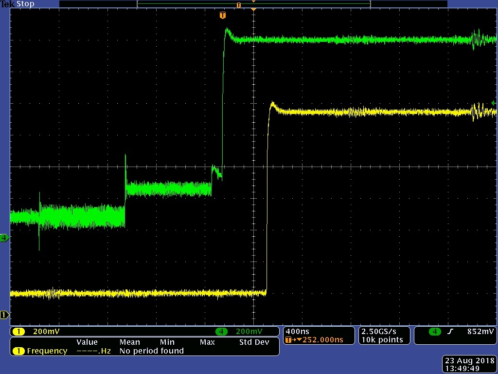
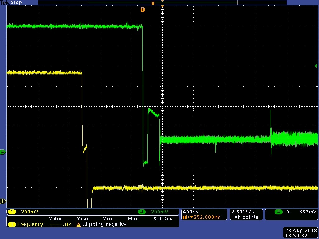
    I believe your clock is working correctly, as you mentioned you do see the transition from LP to HS on CLK. Can you provide the scopeshots of the clock & data on the same plot, have one zoomed in in right before transition into HS mode and another after HS transition?

    The clock should be available right before LS-to-HS transition to capture the data.

    Best,
    Jiashow
  • Hi Jiashow,

    Here are the two scope captures...

    And the LP to HS...

    thanks,

    david

  • Hi David,

    Which waveform is the clock? The green plot looks more consistent like a clock - I don't see any gaps in the waveform like what I would expect for a data plot, but the yellow plot doesn't seen to have any data in HS mode.

    It's strange that for the green plot, there's a step before HS transition and a change in amplitude in the HS mode. Are the signals terminated or just the direct output from the 954?

    Best,
    Jiashow
  • Hi Jiashow,

    The yellow waveform is where the clock should be...  but there is nothing there or as you said "doesn't seem to have any data in HS mode".  I'm not sure what you mean by "gaps in the waveform".

    I agree that the signals in the data stream look strange.  They do not look this way if you look at the data that I send down from the 953's.  I posted an earlier waveform when talking about the strange rolloff of the LP sections of the data.  I will post it again so you can see it.  

    In the scope shot below what you are looking at in the long packets are as follows:

    Each byte below is actually written 480 times... then you start to get the next 480 bytes..  So, first you get 480 bytes of 0xFF then 480 bytes of 0xAA... etc..

    1st long packet --> 0xFF, 0xAA, 0xFF, 0x55, 0xAA, 0x00, 0x55, 0x00. 

    2nd long packet --> 0xFF, 0xFF, 0x55, 0xAA, 0x55, 0xAA, 0x00, 0x00.

    3rd long packet --> 0xFF, 0xAA, 0xFF, 0x55, 0xAA, 0x00, 0x55, 0x00. 

    4th long packet --> 0xFF, 0xFF, 0x55, 0xAA, 0x55, 0xAA, 0x00, 0x00.

    repeat...  So, look at the waveforms below and you can see how the data above correlates to what you see.. 

    Again, how does the clock actually get fed to the CSI-2 CLK pin?

    david

  • Hi David,

    I went into the lab and looked at the plot for CLOCK and DATA on the scope:

    Both the data and clock signals you provided look different from the ones I measured. It seems like there's some output loading issue when you did your measurement, perhaps there is some termination issue as well.

    To your question regarding how clock is fed into the CSI output pins, we have the reference clock going into a PLL to derived the CSI clock output.

    Best,

    Jiashow

  • Hi Jiashow,

    Can you send me the following?

    1) script that you used to setup your 954.

    2) register dump from the 954.

    3) schematic of your 954 circuit including anything connected.

    Remember that I have two boards that are behaving this way and a third setup that is completely different than the two board setups which is also behaving this way.  The boards are driving a FPGA while the 3rd setup has it's 954 CSI-2 outputs connected to a header (no terminations).  I'm not saying that the terminations (as they are right now) may not be a problem but if this was strictly a loading or termination issue I would expect the clock signal to look similar to the data signals.  They do not look similar.  The data signals basically look correct (although a little high) while there is no signal at all on the clock output. 

    I don't believe that this is just a loading problem.  

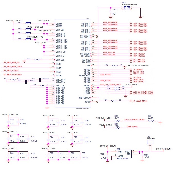
    Also, here is a pic of my schematic.  Please review and let me know if you have any concerns.  I am particularly interested in startup issues as it is looking to me like something is not getting initialized correctly.

    1) uc_cam0_mclk is currently a 24Mhz oscillator.  I originally had it as a 26Mhz oscillator. I have also experimented with no clk at all (just the internal 25Mhz osc)

    thanks,

    david

  • Hi again Jiashow,

    I think this is important...

    I took my third setup which involves three separate boards. 2 953 transmitter boards and a single 954 receiver board. If you remember I said these boards had the same behavior as my more recent single platform boards. This 3 board setup did not have any terminations on the 954 CSI-2 data or clock lines. They simply ran to a connector. (Again, behavior from a scope view was exactly the same) I took the 954 board and dropped a 100ohm differential termination on the clock output. I was thinking that if this was related to loading or termination this should (at a minimum) cause the waveform to change (or the lack of any waveform to show something). The results were exactly the same in regard to the signal on the CSI-2 clock. There is not signal with or without a 100ohm differential termination.

    Please send your schematic, script setup file, and register dump from the working system that you have. If we need to do that privately that's fine.

    thanks,
    david
  • Hi David,

    I used the pattern generator feature from the DS90UB954EVM. You can get the schematics from the user's guide: http://www.ti.com/lit/ug/snlu224/snlu224.pdf  

    The script I ran was very simple and only had 4 lines:

    # CSI cont clk and CSI enable
    board.WriteReg(0x33, 0x01)

    #enable pat gen
    board.WriteReg(0xB0, 0x00)
    board.WriteReg(0xB1, 0x01)
    board.WriteReg(0xB2, 0x01) 

    I am providing the register dump here:

    Reg = 0,0x0000,0x7A
    Reg = 0,0x0001,0x00
    Reg = 0,0x0002,0x1E
    Reg = 0,0x0003,0x20
    Reg = 0,0x0004,0xD3
    Reg = 0,0x0005,0x01
    Reg = 0,0x0006,0x00
    Reg = 0,0x0007,0xFE
    Reg = 0,0x0008,0x1C
    Reg = 0,0x0009,0x10
    Reg = 0,0x000A,0x7A
    Reg = 0,0x000B,0x7A
    Reg = 0,0x000C,0x83
    Reg = 0,0x000D,0xB9
    Reg = 0,0x000E,0x08
    Reg = 0,0x000F,0x7F
    Reg = 0,0x0010,0x00
    Reg = 0,0x0011,0x00
    Reg = 0,0x0012,0x00
    Reg = 0,0x0013,0x00
    Reg = 0,0x0014,0x00
    Reg = 0,0x0015,0x00
    Reg = 0,0x0016,0x00
    Reg = 0,0x0017,0x00
    Reg = 0,0x0018,0x00
    Reg = 0,0x0019,0x00
    Reg = 0,0x001A,0x00
    Reg = 0,0x001B,0x00
    Reg = 0,0x001C,0x00
    Reg = 0,0x001D,0x00
    Reg = 0,0x001E,0x04
    Reg = 0,0x001F,0x02
    Reg = 0,0x0020,0x30
    Reg = 0,0x0021,0x01
    Reg = 0,0x0022,0x00
    Reg = 0,0x0023,0x00
    Reg = 0,0x0024,0x00
    Reg = 0,0x0025,0x00
    Reg = 0,0x0026,0x00
    Reg = 0,0x0027,0x00
    Reg = 0,0x0028,0x00
    Reg = 0,0x0029,0x00
    Reg = 0,0x002A,0x00
    Reg = 0,0x002B,0x00
    Reg = 0,0x002C,0x00
    Reg = 0,0x002D,0x00
    Reg = 0,0x002E,0x00
    Reg = 0,0x002F,0x00
    Reg = 0,0x0030,0x00
    Reg = 0,0x0031,0x00
    Reg = 0,0x0032,0x00
    Reg = 0,0x0033,0x01
    Reg = 0,0x0034,0x40
    Reg = 0,0x0035,0x00
    Reg = 0,0x0036,0x00
    Reg = 0,0x0037,0x00
    Reg = 0,0x0038,0x00
    Reg = 0,0x0039,0x00
    Reg = 0,0x003A,0x00
    Reg = 0,0x003B,0x01
    Reg = 0,0x003C,0x14
    Reg = 0,0x003D,0x6F
    Reg = 0,0x003E,0x00
    Reg = 0,0x003F,0x40
    Reg = 0,0x0040,0x00
    Reg = 0,0x0041,0xA7
    Reg = 0,0x0042,0x71
    Reg = 0,0x0043,0x01
    Reg = 0,0x0044,0x00
    Reg = 0,0x0045,0x00
    Reg = 0,0x004A,0x00
    Reg = 0,0x004B,0x12
    Reg = 0,0x004C,0x00
    Reg = 0,0x004D,0x00
    Reg = 0,0x004E,0x02
    Reg = 0,0x004F,0x00
    Reg = 0,0x0050,0x00
    Reg = 0,0x0051,0x00
    Reg = 0,0x0052,0x00
    Reg = 0,0x0053,0x00
    Reg = 0,0x0054,0x00
    Reg = 0,0x0055,0x00
    Reg = 0,0x0056,0x00
    Reg = 0,0x0057,0x00
    Reg = 0,0x0058,0x1E
    Reg = 0,0x0059,0x00
    Reg = 0,0x005A,0x00
    Reg = 0,0x005B,0x00
    Reg = 0,0x005C,0x00
    Reg = 0,0x005D,0x00
    Reg = 0,0x005E,0x00
    Reg = 0,0x005F,0x00
    Reg = 0,0x0060,0x00
    Reg = 0,0x0061,0x00
    Reg = 0,0x0062,0x00
    Reg = 0,0x0063,0x00
    Reg = 0,0x0064,0x00
    Reg = 0,0x0065,0x00
    Reg = 0,0x0066,0x00
    Reg = 0,0x0067,0x00
    Reg = 0,0x0068,0x00
    Reg = 0,0x0069,0x00
    Reg = 0,0x006A,0x00
    Reg = 0,0x006B,0x00
    Reg = 0,0x006C,0x00
    Reg = 0,0x006D,0x7C
    Reg = 0,0x006E,0x88
    Reg = 0,0x006F,0x88
    Reg = 0,0x0070,0x2B
    Reg = 0,0x0071,0x2C
    Reg = 0,0x0072,0xE4
    Reg = 0,0x0073,0x00
    Reg = 0,0x0074,0x00
    Reg = 0,0x0075,0x00
    Reg = 0,0x0076,0x00
    Reg = 0,0x0077,0xC5
    Reg = 0,0x0078,0x00
    Reg = 0,0x0079,0x01
    Reg = 0,0x007A,0x00
    Reg = 0,0x007B,0x00
    Reg = 0,0x007C,0x20
    Reg = 0,0x007D,0x00
    Reg = 0,0x007E,0x00
    Reg = 0,0x007F,0x00
    Reg = 0,0x00A0,0x02
    Reg = 0,0x00A1,0x0F
    Reg = 0,0x00A2,0x00
    Reg = 0,0x00A3,0x00
    Reg = 0,0x00A4,0x08
    Reg = 0,0x00A5,0x19
    Reg = 0,0x00B0,0x00
    Reg = 0,0x00B1,0x01
    Reg = 0,0x00B2,0x01
    Reg = 0,0x00B3,0x08
    Reg = 0,0x00B4,0x25
    Reg = 0,0x00B5,0x00
    Reg = 0,0x00B6,0x18
    Reg = 0,0x00B7,0x00
    Reg = 0,0x00B8,0xFC
    Reg = 0,0x00B9,0x33
    Reg = 0,0x00BA,0x83
    Reg = 0,0x00BB,0x74
    Reg = 0,0x00BC,0x80
    Reg = 0,0x00BD,0x00
    Reg = 0,0x00BE,0x00
    Reg = 0,0x00BF,0x00
    Reg = 0,0x00D0,0x00
    Reg = 0,0x00D1,0x43
    Reg = 0,0x00D2,0x94
    Reg = 0,0x00D3,0x0F
    Reg = 0,0x00D4,0x60
    Reg = 0,0x00D5,0xF2
    Reg = 0,0x00D6,0x00
    Reg = 0,0x00D7,0x02
    Reg = 0,0x00D8,0x00
    Reg = 0,0x00D9,0x00
    Reg = 0,0x00DA,0x00
    Reg = 0,0x00DB,0x00
    Reg = 0,0x00DC,0x00
    Reg = 0,0x00DD,0x00
    Reg = 0,0x00DE,0x00
    Reg = 0,0x00DF,0x00
    Reg = 0,0x00F0,0x5F
    Reg = 0,0x00F1,0x55
    Reg = 0,0x00F2,0x42
    Reg = 0,0x00F3,0x39
    Reg = 0,0x00F4,0x35
    Reg = 0,0x00F5,0x34
    Reg = 0,0x00F8,0x00
    Reg = 0,0x00F9,0x00
    Reg = 0,0x00FA,0x00
    Reg = 0,0x00FB,0x00

    Do you have a 954EVM that you could test this on? It's possible this could be a board issue.

    Best,

    Jiashow

  • Hi Jiashow,

    Thank you for the information.

    I have been looking at my power rails, pdb signal, and refclk signal relationships at power up... I am using VDD_SEL = low and so the datasheet shows that I have nothing to do with when VDD11 comes up... but, when I look at the Power_up_Sequencing (in the datasheet) for when VDD_SEL = high it shows the VDD11 coming on line after VDD18 & VDDIO but before PDB goes high. I was therefore expecting VDD11 to go high prior to PDB going high in my situation of VDD_SEL = low... but that is not what is happening. In my system VDD11 does not go high until it sees PDB go high.

    This seems odd to me since in one case (VDD_SEL = high) it was important to pull VDD11 high prior to PDB going high.. but not in the other case.. Is this right?

    I can say that after PDB and VDD11 are high that pulling PDB back low does not affect VDD11.

    Can you offer some advice on this?

    thanks,
    david