Part Number: DS32EL0124
Hi,
Our customer used DS32EL0124 for FPGA high speed data transmission but when he try to follow DS32EL0124 DS page17 "reading a register issue description" to programming their FPGA code but slave can't reply corresponding register while he write.
The DS of reading a register issue description as below:
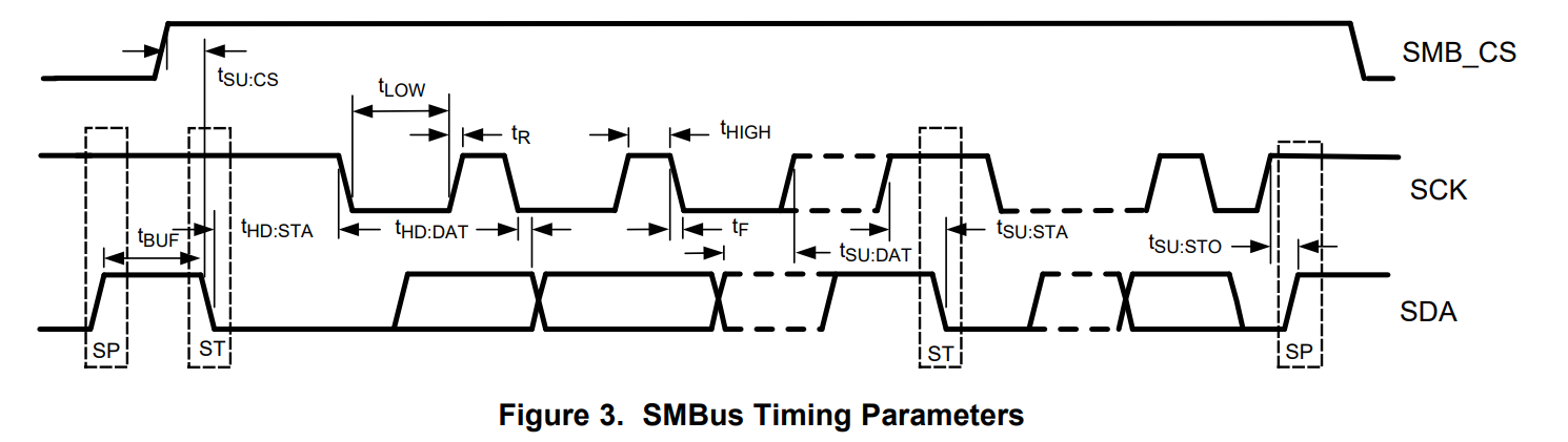
1. The Host (Master) selects the device by driving its SMBus Chip Select (SMB_CS) signal HIGH. 2. The Host drives a START condition, the 7-bit SMBus address, and a “0” indicating a WRITE. 3. The Device (Slave) drives the ACK bit (“0”). 4. The Host drives the 8-bit Register Address. 5. The Device drives an ACK bit (“0”). 6. The Host drives a START condition. 7. The Host drives the 7-bit SMBus Address, and a “1” indicating a READ. 8. The Device drives an ACK bit “0”. 9. The Device drives the 8-bit data value (register contents). 10. The Host drives a NACK bit “1”indicating end of the READ transfer. 11. The Host drives a STOP condition. 12. The Host de-selects the device by driving its SMBus CS signal Low
Could you please share the DS32EL0124 SMBus clock waveform which follow the description as above.
And customer can follow the waveform to programming their FPGA code to generate right communication data clock.
Thank you.
Warm Regards,
Kevin Lin