


Other Parts Discussed in Thread: TLK105
Hi,
I'm working on an EtherCAT design spin I inherited from another engineer which previously had the TLK105 PHY on board. I'm in the process of migrating it to the DP83822 since I've gathered from other posts on e2e that the TLK105 is NRND, and the DP83822 also seems to offer some worthwhile enhancements.
In combing through the datasheets EVM docs, and layout guides, I keep encountering this combination of bypass caps on the part's power rails:
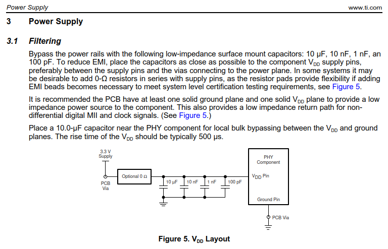
This particular snippet is from the "TLK1XX Design and Layout Guide" (SLVA531A). To be blunt: this PDN leaves a lot to be desired. In my view, a simplistic combination of caps spaced one decade apart in value like this is always bad practice with low-impedance MLCCs because of the large anti-resonant impedance peaks such a combination produces. Furthermore, this kind of network contradicts specific design advice from TI given in several other design resource documents (e.g. SWPA222A "Power Delivery Network Analysis" or section 2.4 "Decoupling Capacitors" of SCAA082A). I realize TI is a sprawling organization and probably not all of the engineers who author datasheets and app notes are aware of everything put out by the company as a whole, but I see this kind of bad advice given frequently and felt the need to question it.
Here a plot of impedance vs frequency for this recommended network (black trace, and horizontal black line shows the DP83822's target impedance):

First, some caveats: this is a pretty simple sim I threw together in a few minutes to illustrate my point, and it doesn't model the impedance of any power plane distributed capacitance. I also had to make an assumption about the 10uF cap's inductance and ESR, but I think I'm reasonably close based on experience. This said, there's a lot that could be done to improve this network. As a quick example, I also modeled converting all three 0402 caps to .1uF parts (red trace) or to 1uF parts (green trace), which avoids the high-frequency resonances. Arguably, the 3x .1uF network is better in almost all respects, unless TI was shooting for low Z at the three specific impedance minima shown in the graph, but that seems unlikely to me. Adding some damping in the form of resistors or using controlled ESR ceramic caps would certainly help. There's a lot more written about this subject from people like Brooks, Archambault, Bogatin, Ott, Ritchey, and other EMC / PCB layout gurus.
Can anyone at TI comment on why this specific network was recommended? I realize the answer may come down to something like "it worked, it's inexpensive, and it passed EMI tests." That might be fine for some, but I'm shooting for a higher standard of performance. Of course one could pour an inordinate amount of time and effort into improving this single aspect of the design, and such efforts must always be balanced with performance yield, but based on experience I think this network could be improved significantly with minimal effort.
Thanks,
Josh
