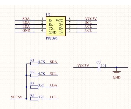
This thread has been locked.

If you have a related question, please click the "Ask a related question" button in the top right corner. The newly created question will be automatically linked to this question.

P82B96: Communication anomaly

Part Number: P82B96

Customers is developing HMDI2.0 cable. DDC buffer uses P82B96. Current tests have found that when Philips players are interconnected with SONY KD49X7500E televisions, the televisions cannot recognize the players.Other combinations are now working properly, and the P82B96 on the TX side can be replaced with the  NXP P82B96 (Work normally). The length is 8-40 meters, and the SCL frequency is 100kHz.

No obvious abnormalities were found in testing the SDA waveform. What is the reason for this anomaly?

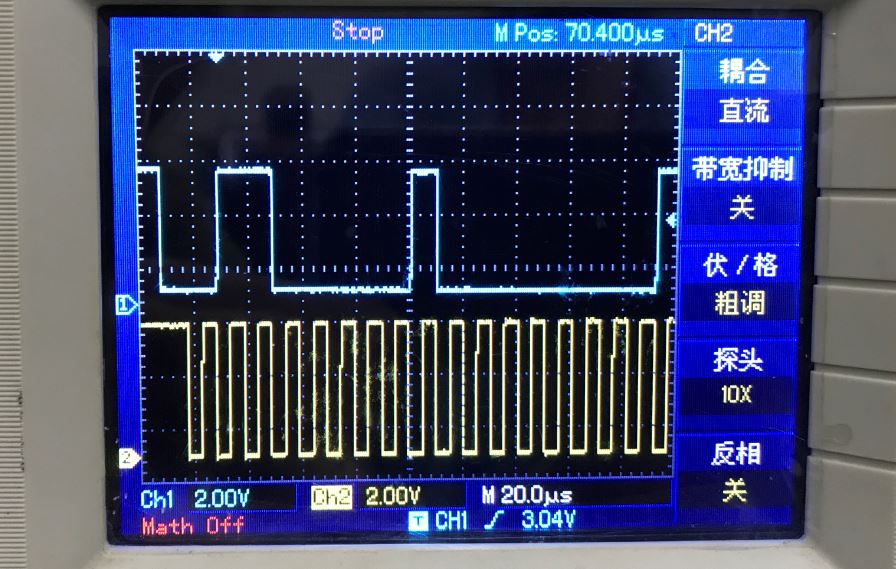
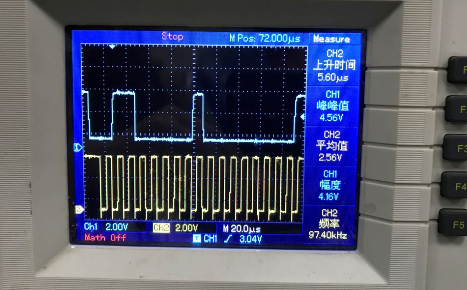
TI P82B96  BULE input signal   YELLOW output signal

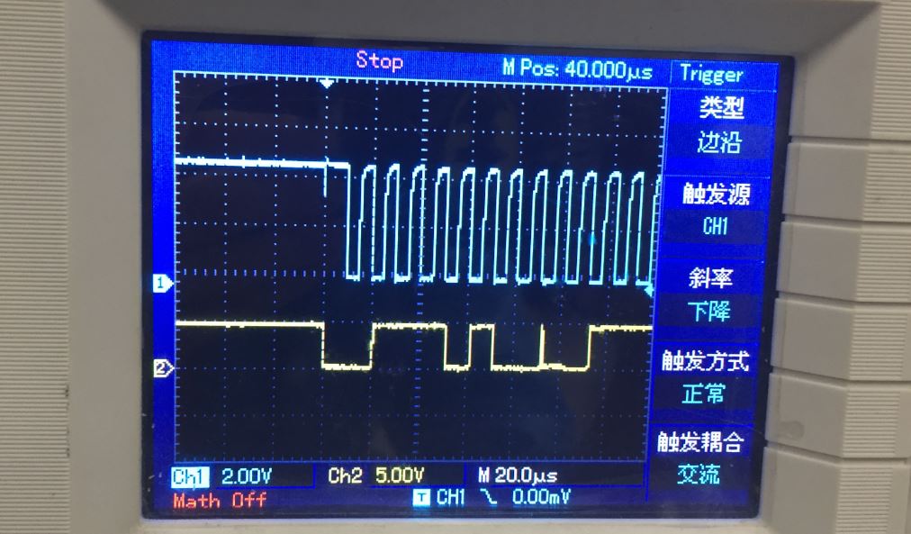
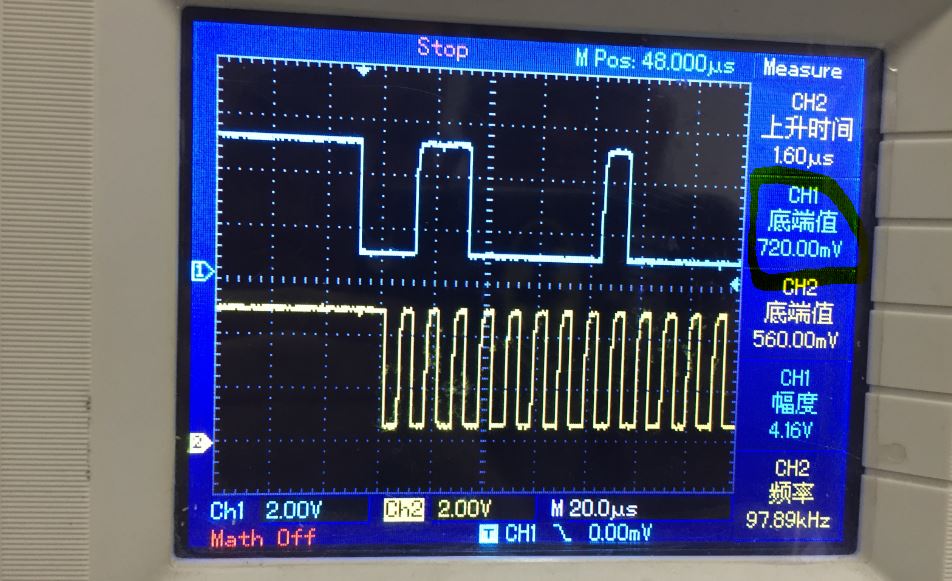
NXP P82B96  BULE input signal   YELLOW output signal

  • Hello Shuang,

    I want to confirm, you are using two P82B96 devices, one for transmitting and one for receiving:

    master/slave->P82B96-----long cable-----P82B96---<--master/slave

    I am not as familiar with DDC2B but looking online it looks like it communicates using a protocol similar to I2C so:

    Are you seeing an ACK when you read/write to the slave?

    How about when the master is reading, does it send an ACK back correctly to the slave when it wants to read more data?

    You posted pictures of the data line which looks okay to me, I don't see any issues with it. Can you post the clock lines?

    Does our device work at smaller distances or does it fail at all distances?

    Is it possible that our P82B96 devices could have been damaged? If you replace our device with a new one, does it work again?

    Can you also post scope shots of both clock and data on the transmission end and another of both clock and data on the receiving end?

    Thanks,

    -Bobby

    freqinput()==1

  • Hi  Bobby,

    master/slave->P82B96-----long cable-----P82B96---<--master/slave

    YES

    I am not as familiar with DDC2B but looking online it looks like it communicates using a protocol similar to I2C so:

    Are you seeing an ACK when you read/write to the slave?   See picture below.

    How about when the master is reading, does it send an ACK back correctly to the slave when it wants to read more data?

    You posted pictures of the data line which looks okay to me, I don't see any issues with it. Can you post the clock lines?

    TX  SDA &SCL

    RX  SDA &SCL

    Does our device work at smaller distances or does it fail at all distances?

    We test 8m and 30m all fail

    Is it possible that our P82B96 devices could have been damaged? If you replace our device with a new one, does it work again?

    I can use this cable connect  X-BOX and sony TV well. If change to PHILPS Blu ray player ,the fail rate is 400/400.  If replace to NXP part ,it works well.  

    What causes this kind of general problem? Is there any way to solve it?

    NXP PART TX  SCL &SDA      (There are images on TV.)

  • Hey Shuang,

    Your first two pictures with our device show that the slave is NACKing. This means there is something going on with the slave device. You can see the ACK in the NXP image where SDA goes high for a little then gets pulled low by the slave on the 9th clock cycle.

    I would like to verify, Is the first image and second image you posted measured like this?:

    ----------

    Something about your first image looks strange, the rising edges on both the clock and data line look very fast. What is the pull up resistor on SDA/SCL of TX side?

    The second image shows that the clock line is swinging below below 0V by almost -1V. Our device is spec'd for a maximum of -0.3V so this kind of undershooting can damage our device.

    Your VoL on the TX side looks large on the data line, can you measure this?.Your VoL on Rx side does not look right, there should be a shift of 800mV or so but it looks like it is holding on to GND, please measure this as well.

    Thanks,

    -Bobby

  • Hi Bobby,

    I would like to verify, Is the first image and second image you posted measured like this?:  YES

    ----------

    Something about your first image looks strange, the rising edges on both the clock and data line look very fast. What is the pull up resistor on SDA/SCL of TX side?  

    For Rm&Rs is 4.7kohm  for Rb is 330ohm    both pull up voltage is 5V.

    The second image shows that the clock line is swinging below below 0V by almost -1V. Our device is spec'd for a maximum of -0.3V so this kind of undershooting can damage our device.

    I think this is cause by poor contact with reference ground.

    Your VoL on the TX side looks large on the data line, can you measure this?.Your VoL on Rx side does not look right, there should be a shift of 800mV or so but it looks like it is holding on to GND, please measure this as well.

    TX vol 400mv

    RX  vol 720mv

  • Hey Shuang,

    400mV and 240mV in your TX picture look fine, this is below the required 600mV ViL for the device.

    In your second picture, VoL of the clock at 560mV does not sound right to me, VoL on yellow should be something like 700mV+.....

    Do you know what the ViL of your slave is? Also if we compare SDA of the RX side of NXP's P82B96, what is the VoL? I am wondering if NXP's VoL is lower than ours and the slave does not accept 720mV as a low.

    Other than this, I do not see anything wrong with the signals. Are you able to post the schematic of our device and the slaves attached to our devices? If this is sensitive information, we can discuss over email: duynguyen@ti.com

    Thanks,

    -Bobby

  • Hi Bobby,

    400mV and 240mV in your TX picture look fine, this is below the required 600mV ViL for the device.

    In your second picture, VoL of the clock at 560mV does not sound right to me, VoL on yellow should be something like 700mV+.....

    TX Vol SDA- SCL 400mv-240mv =160mv    RX Vol SDA- SCL 720mv-560mv =160mv   so I think the test result is reasonable.

    Do you know what the ViL of your slave is? Also if we compare SDA of the RX side of NXP's P82B96, what is the VoL? I am wondering if NXP's VoL is lower than ours and the slave does not accept 720mV as a low.

    I can see NXP RX SDA is lower, I want to know what can effect the VOL Voltage.  External devices or chips themselves?


  • Hello Shuang,

    "TX Vol SDA- SCL 400mv-240mv =160mv    RX Vol SDA- SCL 720mv-560mv =160mv   so I think the test result is reasonable."

    The difference between VoL of Data and Clock should be unrelated to each other so subtracting the difference from each other will not tell us anything. What I am saying is RX VoL on the clock seems lower than what I expect it should be.

    From the schematic you are showing me, 5V/4700ohm give us about 0.2mA of current.

    You can see above that if you have about 0.2mA of current then the minimum VoL should be is 0.67V. Your your VoL is 0.56V which is below the minimum.

    "I want to know what can effect the VOL Voltage.  External devices or chips themselves?"

    If VoL is larger than ViL of a slave, then the slave will never see a logic low. This effects external devices in this way. <-- This is my concern and I am wondering if this is the reasonw why NXP's works and ours doesn't. The signals from TX to Rx look like they are at least sending and receiving the data properly but the slave does not recognize or see the signal.

    Can you provide what the slave device is, I want to look and see what the ViL requirement for it is.

    VoL also needs to be larger than ViLc of this device otherwise it could latch the bus low. From your scope shots, this doesn't seem to be the case.

    Thanks,

    -Bobby

  • Hi Bobby,

    The slave device is Sony TV  KD-49X7500E

  • Hey Shuang,

    The TV is an end equipment. What I am asking to know is what is the I2C slave device connected to the P82B96 (inside of the TV).

    Thanks,
    -Bobby