This thread has been locked.

If you have a related question, please click the "Ask a related question" button in the top right corner. The newly created question will be automatically linked to this question.

Damaged output leg

Part Number: AM26LV31E
Other Parts Discussed in Thread: AM26LV32E, , AM26LV32

Hello,

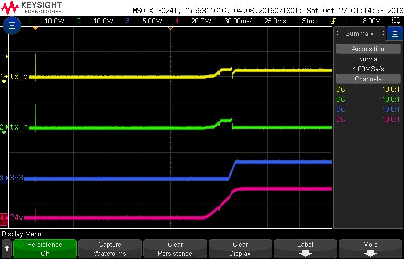
I am troubleshooting a failure in a design where the AM26LV31E driver is not producing a differential signal on the output.  The failed leg of the output is a duplicate of the other leg.  Both differential outputs are switching, but the outputs are the same.  The driver interfaces with a AM26LV32E receiver on another PCB.  Both the driver are receiver are running at 3.3V from switching power supplies on each board.  The board with the driver is hot swappable in the system, using a hot swap controller that enables its switching power supply.  I'm looking for any advice in trying to help isolate this failure mode. 

Thank you

  • Andrew,

    If termination is populated on the bus, then you would see both halves of the differential signal switching "in phase" if one of the lines was acting as a high-impedance. This could be the case if there is a poor solder connection from the pin to the PCB (or anywhere else in the path of the signal, such as a connector), or it could be the case if the unit is damaged in such a way that one half of the output had failed open. The first option is generally more likely so I would check that first. You could do this by probing the output pin directly (if possible) or by reflowing the PCB. Once you verify that is is not a connection issue, then you could check for damage to the IC by swapping it to a new PCB and seeing if issues remain or by taking some pin input resistance measurements and comparing them to a known-good unit.

    Regards,
    Max
  • Max,

    The failures I'm seeing in this design result in the differential signal switching "in phase" as you've described.  It doesn't appear to be a connectivity or termination issue.  I've removed and replaced the damaged AM26LV31E drivers which has fixed all the units affected.  Are there any specific conditions I should be looking for that would cause an AM26LV31E to fail and have one leg of the differential output damaged?  I'm not seeing any overshoot in the device's 3.3V power supply on startup or any transients that would exceed the absolute maximums of the device, however I haven't been able to obtain a failure while monitoring anything.  In this application, the receiver which is an AM26LV32E is on another pcb with power applied prior to the pcb with the driver being inserted into the system and powered up through use of a hot swap controller.  Both pcbs are powered off their own 3.3V switching power supplies.

    Thanks

    Andrew

  • Andrew,

    Do you know when the failure might have occurred? For example, was it prior to first power-up (suggesting an issue at assembly or handling)? Or, did it occur after connecting power or data cables (suggesting possibilities like overshoots on power-up or hot plugging transients)? Or, did it occur after the system had functioned normally for some time (suggesting environmental stresses like ESD)? This could help narrow things down.

    I'd say that generally speaking the most common cause of "in situ" damage to devices like this is the coupling of overstress transients (ESD, etc.) to the differential signal pins via an external connector. The AM26LV31E does have fairly strong internal transient protection, though, and so I'd be a little surprised to see it be damaged via this mechanism unless you had reason to believe the system had been exposed to more extreme stresses.

    You mentioned that each device was powered by an independent 3.3-V supply. Do these supplies share a common ground reference (e.g., via a dedicated ground wire in the cable used to connect the nodes)? Or could there potentially be an offset in ground potentials between the nodes? If there were a suitably high ground offset then it may result in voltages at a given node that exceed the absolute maximum pin ratings.

    Also, based on your confirmation that there are no connection issues I am assuming one half of the differential output pair has failed open. To make sure we are on the right track, though, could you try measuring the output waveforms when line termination is removed? In that case I would expect to see one line toggling and one line static (or maybe toggling at a significantly lower level due to parasitic coupling between the lines). If you still see both halves of the differential output toggling even with no low-resistance connection between them then we should revisit our assumed failure mechanism.

    Regards,
    Max
  • Hi Max,

    Failures are occurring on units after running anywhere from days, up to two years.  Hot swaps occur daily during normal use.  The device that is getting damaged is on the PCB that is regularly hot swapped.  It's the driver side of the RS-422 interface.  There is a common ground between the two PCBs, which is made through a blind mate interface.  I suspect the damage is due to the hot swapping of the PCB with the driver on it and there could be a momentary ground potential difference, but I have not verified this or reproduced it yet.

    I verified on a failed unit, without a termination resistor, the damaged output is toggling at a much lower level in phase with the output that is working normally.  As you mentioned, this appears to be just the parasitic coupling between the lines.

    I measured a failed AM26LV31E for resistance from the differential outputs to ground.  On a failed unit I see 304k to ground on the failed output and 274k to ground on the functioning output.  A working unit has 276k to ground on both output legs to ground for comparison.  So it appears the resistance to ground went up by about 30k ohm on the failed output. 

    I'll be taking some measurements to try to look for a ground potential difference.

    Thanks,

    Andrew

  • Andrew,

    The resistance difference is relatively small, but I suppose this could be the case if just some portion of the internal circuitry had failed open. Resistance measurements are convenient but not always a perfect way for diagnosing failures on active devices. If you have a way of performing an I/V curve trace that may help us better understand the nature of the failure. Or you could try returning the IC via your distributor for failure analysis.

    Please keep me posted as you progress through the measurements. Sometimes having an oscilloscope probe connected to the bus IOs of a transceiver while plugging and unplugging a cable can reveal some unexpected transients - that may be one way to catch potential failure sources like momentary ground shifts, discharges from cables, accidental shorts to power supplies (e.g., due to connector misalignment), etc.

    Max
  • Hi Andrew,

    Just checking in - have you had any luck in debugging this failure further?

    Regards,
    Max
  • Hi Max,

    I am currently taking measurements with a scope.  I am seeing some transients on the RS-422 driver lines during system power up, prior to even when the device has been enabled with VCC.  The transients last for about 5us and can go up to 10V, average pulse width of about 150 ns.  Systems are power cycled at least daily.  If the AM26LV31E gets transients he on the driver's diff pair outputs like this, prior to being powered up, can that be ultimately causing some of our failures?  Please see the attached traces TX_P, and TX_N.   This is what is on these interfaces about 180 us prior to the driver even getting VCC.  Other loads in the system are coming on at this time and have large inrush currents.  I see on the device datasheet an absolute max of 6V.  Do you have any information about what would happen to an unpowered driver with transients as shown?

    I am also looking into the behavior of these lines during hot swap.

    Thanks,

    Andrew

  • Max,

    I'm considering adding a TVS to these lines based on the transients I've measured prior to the device power up. I've included some details in the reply below.

    Thanks,
    Andrew
  • Hi Andrew,

    Thanks for the scope plots. I do believe that repeated exposure to +10 V could degrade these devices and result in eventual failure, but I will loop in another one of my colleagues to try to confirm this (I am out of the office at the moment). If this is the case, though, TVS diodes would make sense as a solution as long as you could find one that would clamp the 10 V signals without limiting normal operation of the transceiver.

    Do you know the source of these disturbances when the system is powered up?

    Max
  • Hi Max,

    Thanks. Yes the repeated exposure was what I was concerned about as well. The exposure to these transients would be prior to the device getting VCC, by about 180 us. I'm trying to determine the exact source of these disturbances, but I suspect that it is related to VFDs turning on and starting two 3 phase motors in the system. The transients occur right at switching on the main disconnect for the system, which starts the VFDs and motors. The cabinet also has a switching power supply, 24V, which is used by the PCB where this 422 driver is, the 24V goes through a hot swap controller and filtering, then to a switching power supply to generated the device's 3.3V VCC. I think some of the transients are from radiated noise during the turn on, as I've had some success at least partially attenuating the transients with improved shielding of the 422 pair. I'm currently looking into adding TVS and small series resistors on the driver's output as I've seen in some other posts on here. I'm considering the CDSOD323-T03 or CDSOD323-T05. I'd like to clamp transients above 6V if possible, but allow for normal operation at 3.3V.

    Thanks,
    Andrew
  • Max,

    Here's a larger time scale view of the turn on and transient event.

  • Andrew,

    I tested a couple of parts in lab by shortening TX_P and TX_N pins to 10V supply (individually or simultaneously) for 10s of seconds. But so far I haven't seen a device failure. Can you confirm your ground connection during your tests? Thanks,

    Hao
  • Hao,

    Is that measurement with no VCC applied to the part?

    My scope probe ground leads are as short as I can get them at the moment, returning to the driver ground plane. Perhaps I could sketch up a diagram of the setup if needed. This device runs off a 3.3V switching P/S with a 24V input that comes from a hotswap controller. Ground is common on everything in the PCB with the 24V return. The 24V return does come through a blind mate interface, which is engaged, otherwise it is all hard wired back to an industrial control panel which runs off 480 3 Phase and has a 24V switching P/S inside of it. The control panel also has the VFDs I mentioned that are starting up motors which I suspect there to be transients from.

    The parts you tested seem robust to handle 10V, I assumed that was so much more than the 6V abs max that it would cause damage. Do you think all parts would behave the same?

    Thanks,
    Andrew
  • Andrew,

    I didn't put Vcc to the part in my tests. Thanks for your explanation on your setup. We will brain storm tomorrow. The damage caused by over stress voltage could only be described statistically. Higher voltage and longer time will generate more damaged parts over large samples. Unfortunately this data is very hard to characterize.

    Regards,
    Hao
  • Thank you Hao.  I appreciate the support.

    Andrew

  • Andrew,
    We discuss your setup internally. Although I didn't see 10V voltage damage the output pins of the devices I tested, we cannot conclude it's not harmful to the devices (anyway it's above 6V abs max). I think the best practice would be filtering the spike of the voltage during transients to make it lower than the abs max. If you still find the damages after the fix, we could see what else can be improved then.
    Regards,
    Hao
  • Hao,

    Thanks.  I am going to modify a board and install TVS on the data lines.  I will trial CDSOD323-T03 and CDSOD323-T05 unidirectional TVS.  The -T03 may be too low of a Vwm at 3.3V.  But the -T05 has a Vbr of 6.0V and a Vclamp of 9.8V.  Do you have any recommended TVS parts or circuit implementation for the AM26LV31E/AM26LV32?  I'd like to trial and determine the appropriate TVS circuit, then will likely respin the PCB if we obtain the desired improvement.

    Regards,

    Andrew

  • Andrew,

    You may want to try SMBJ3V3 or PESD3V3.

    Regards,

    Hao

  • Hi Andrew,

    Did the addition of the TVS on the data lines seem to help?

    Regards,
    Max