This thread has been locked.

If you have a related question, please click the "Ask a related question" button in the top right corner. The newly created question will be automatically linked to this question.

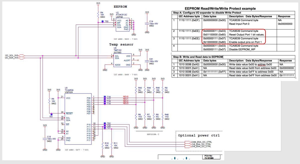
TCA9539: I want to enable EEPROM(AT24C512C).

Part Number: TCA9539

[Figure Table]

I want to enable EEPROM(AT24C512C).
For now, it is disabled for Writing fW because of TCA9539 so I cannot get a precise information from EEPROM.

1. Please let me know how to enable EEPROM. (The order of putting Data to EEPROM, How to set up.)

Also as you can see No.2 in [Figure table], there's a 2 Data bytes. How can I understand that?
Ex. is that right? Address : 0x03 / Data : 0x60
Ex. or is that right? Data : 0x03 / Data : 0x60

2. Please give me a datasheet of TCA9539 which consist of Register map for FW tuning.

  • Hello Kim,

    "Also as you can see No.2 in [Figure table], there's a 2 Data bytes. How can I understand that?"

    I assume you are talking about from your picture. After sending the slave address with a write bit, the first byte sends the command byte (register you want to write to), the second byte is the data you write into that register

    "Ex. is that right? Address : 0x03 / Data : 0x60
    Ex. or is that right? Data : 0x03 / Data : 0x60"

    Example: Address(0x77)-->command byte (0x03)--> Data (0x60)

    I assume you are just trying to pull P15 (the pin tied to WP) low.

    If that is correct then in step #2 the data should be 0b XX0X XXXX. So 1101 1111 would work but so would 0000 0000.

    "2. Please give me a datasheet of TCA9539 which consist of Register map for FW tuning."

    I am unsure what you mean by this. Table 3 in the datasheet shows the command bytes (register address) you can program. Tables4, 5, 6, and 7 show the default states and beneath them describe what they do.

    If you have further questions, do not hesitate to ask.

    Thanks,

    -Bobby