This thread has been locked.

If you have a related question, please click the "Ask a related question" button in the top right corner. The newly created question will be automatically linked to this question.

TMDS181: TMDS181 SI(Signal integrity) test fail

Part Number: TMDS181

Dear Support

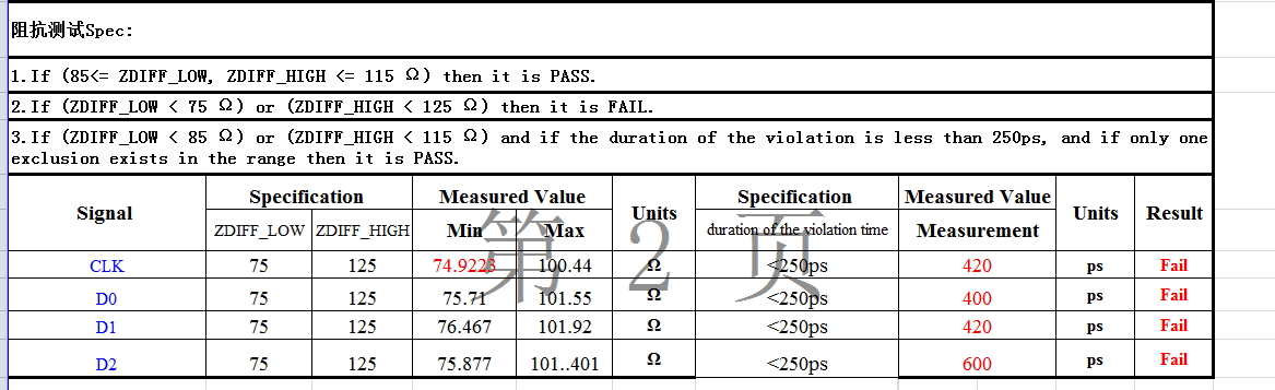
The customer feedback TMDS181 on the SI test failed

Do you have any suggestion?

The PCB setup below

1. impedance 95 ohm.

2. differential pair spacing is about 20MIL at present, and 30mil or 4 times linewidth can not be applied in practice.

3. The difference between the differential lines is +/-5mil. The total length did not exceed 2 Inch.

4. the element is symmetrical on the differential line.

5., there are suitable ESD devices (ESD8004MUTAG) on the signal line.

Please see the enclose about PCB and Schematic

PCB.pdf 2248.TMDS181.pdf

  • Seven

    Do you have the bare board impedance measurement result that you can share?

    Please try to remove the ESD component and see if it helps with passing the impedance test.

    The layout file is not complete, but looking at it, here are my questions.
    1. Are you routing the signal on the top layer? It looks like you are using a through-hole connector. If this is the case, you need to rout the signal on the bottom layer to make the through-hole pin to be part of the transmission, preventing the through-hole pin from acting as a stub in the signal transmission path.
    2. It looks like you are changing the HDMI differential trace from one layer to another layer. If this is the case, do you have the GND via next to the signal via for the current return path?
    3. Do you have solid reference plane underneath the HDMI differential trace? Are they GND or power reference plane?

    Thanks
    David