This thread has been locked.

If you have a related question, please click the "Ask a related question" button in the top right corner. The newly created question will be automatically linked to this question.

PCA9306: Issue related to VREF2 resistor value

Part Number: PCA9306

Hi team,

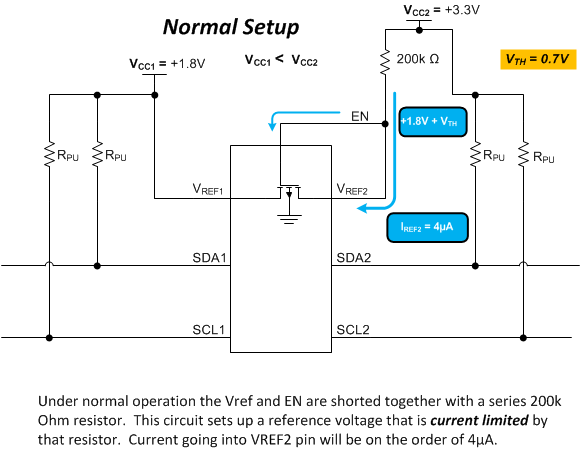
We have used PCA9306 Level Translator in our one of project as per below Schematics.

We are converting 3.3V level to 1.8V level and at 1.8V side IMU Chip is connected.

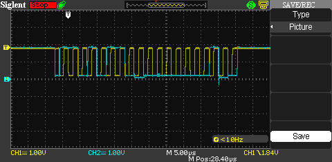
There are few boards on which when I am connecting 100R resistor instead of 200K then only Level Translator works Correctly & we are getting the IMU Slave data Properly.

We have tried various resistors like 10K, 100K, 1K, 4.7K but nothing Works. When I replaced the 100K with 100 Ohm resistor then It starts working & I am getting the Correct IMU data.
I have also tried with replacing the level translator and IMU also but still it doesn't work , when we tried with 100 Ohm it's working fine.
- What this 200K Resistor cause & why is it Impacting on the Performance?
- We want to know the exact reason that why is it working only with 100 Ohm & Lesser value? 
- Do you see any Risk if we change the 200K by 100 Ohms on all the boards?

Waiting for your quick response.

Thanks and Regards,

Margisha Dave

  • Hello Margisha,

    Your questions about the 200k ohm resistor is discussed in this thread:

    "What this 200K Resistor cause & why is it Impacting on the Performance?"

    As the link above discusses, the 200k ohm resistor is there to limit the current while establishing a reference voltage to other circuitry in the device.

    Request #1: please measure the voltage of the enable pin on an o-scope and provide the image for us to check

    Request #2:please also measure Vref1 on an o-scope and provide image

    "Do you see any Risk if we change the 200K by 100 Ohms on all the boards?"

    From what I see in your schematic, going from 200k ohms to 100 ohms will give a current between Vref1 and Vref2 of about 15mA. To our device there should not be any damage through the FET between Vref1 and Vref2. Only additional power consumption.

    "We want to know the exact reason that why is it working only with 100 Ohm & Lesser value? "

    Changing the resistor value will only affect the current between Vref1 and Vref2. I've seen one case where Vref1 was supplying it's voltage using an LDO and the LDO would lose regulation because it was a high impedance source and could not sink the leakage current between Vref2 and Vref1. We were able to resolve this by providing a path to GND from Vref1 using a pull down resistor around the range of 150k ohms. I'm not sure if this is the same case for you until I see what Vref1 and the enable voltage are.

    Request #3: Can you also provide scopeshots of what the I2C bus look like on side 1 and side 2 when you use resistor values that do not work?

    thanks,

    -Bobby

  • Hi Booby,

    Thanks for your Kind response.

    Please fine the attached images;

    Request #1: please measure the voltage of the enable pin on an o-scope and provide the image for us to check -- Voltage_EN.jpg V =3.36V


    Request #2:please also measure Vref1 on an o-scope and provide image -- Voltage_Vref1.jpg V = 1.8

    Request #3: Can you also provide scopeshots of what the I2C bus look like on side 1 and side 2 when you use resistor values that do not work? - I will send you this soon.

    As you said:

    "We were able to resolve this by providing a path to GND from Vref1 using a pull down resistor around the range of 150k ohms. I'm not sure if this is the same case for you until I see what Vref1 and the enable voltage are."

    - I also want to understand this case in detail . As in how you provided grounding path and how it is affecting the working of IC.

    Thanks

    Margisha

  • Hello Margisha,

    The second image of Vref1 looks good.

    Something is wrong with the enable pin voltage. This voltage should not be 3.3V, it should be around 2.4V~2.5V

    Please verify you are probing the right spot:

    If the enable voltage is 3.3V then this device will not work properly.

    Can you provide a picture of the layout of the PCB for PCA9306, I would like to verify Vref2 and enable pin are shorted together and go to the two 100k series resistors.

    Please also verify Vref2 pin and the enable pin are shorted together on the PCB by doing a continuity check with a DMM.

    " I also want to understand this case in detail . As in how you provided grounding path and how it is affecting the working of IC."

    The GND path was from Vref1 to GND with a resistor at around 150k ohms. We found that the Vref1 voltage was shifted up to something like 2.5V when it was intended to be 1.8V, this in turn shifted the enable voltage higher and did not provide translation from side 1 to side 2 and vice versa.

    The pull down resistor on Vref1 provided a path from the leakage current from Vref2 to Vref1 to go to rather than build up voltage on the LDO's output. This allowed the LDO to regulate it's voltage correctly.

    I do not believe this is your problem because Vref1 is 1.8V steady.

    -Bobby

  • Hi Bobby,

    There were some misunderstanding from my end. Please find the image for EN pin below and the voltages are ~2.7V

    Request #3: Can you also provide scopeshots of what the I2C bus look like on side 1 and side 2 when you use resistor values that do not work? --- Please also find the image of clock and data at side 1 and side 2 of the level translator while in not working condition.

    Image 1 - SDA_SCL_3V3

    Image 2 - SDA_SCL_1V8

    I got your point regarding the LDO regulation and exactly that is not our case as you also observed the stable 1.8V at Vref1.

    Please provide your valuable observations for our case.

    Thanks

    -Margisha

  • Hey Margisha,

    Your new enable pin voltage looks good.

    Your scope shots of the I2C signal look good. Every 9th clock cycle we also see the ACK bit go low which means that the slave is seeing the signal and responding, also from the master's side the master also sees the slave ACK. The voltages have been translated from one side to the other. To me it looks like PCA9306 is doing its job. There is no indication the I2C signal is bad.

    What is the slave device?
    Can you describe what the slave you are communicating with is supposed to do? (What are you defining as a failure?)

    Thanks,
    -Bobby
  • Hi Bobby,
    We are communicating with IMU as a slave device. We are using ICM20948 IMU unit. As it it IMU it should give data on it's position change as but it's not the case for our condition. But when I reduce the enble pin resistor to 100E I am able to get data of IMU. I can't understand this why this kind of behavior is happening if Level Translator is working fine then why the change in EN pin resistor of level translator affect my IMU data output.!?

    Thanks
    - Margisha
  • Hello Margisha,

    "it should give data on it's position change as but it's not the case for our condition. "
    For this I would assume to get data from the slave you would need to perform a read transaction with the slave. From the image I see above, the master is sending a write transaction to the slave.

    Here is what I see:
    1) Start condition
    2) Master sends address: 0x6B with a write bit
    3) slave ACKs
    4) Master sends the command/data byte: 0x01
    5) slave ACKs
    6) Stop condition

    Request: Can you please send scope shots of the read transaction where you try to get the position data from the slave?

    Thanks,
    -Bobby