This thread has been locked.

If you have a related question, please click the "Ask a related question" button in the top right corner. The newly created question will be automatically linked to this question.

DP83848C: interfacing dp83848C in MII mode with STM3240G-EVAL

Part Number: DP83848C

Hello all,

 i am using stm3240g-eval  development board and together with dp83848C and I am trying to bring up the Ethernet module.

I was unable to send and receive data using the MII interface. 

the following configurations has been set.

MII mode

PHY address - 0x01

Auto.negotiation - Enabled

speed - 100Mbps

with above configuration, in basic mode status register bit 5 is not set.

is there any internal clock of 25MHZ to the dp83848C??.

Kindly help me overcome the above problems.  

Best Regards,

Siva

  • Hi Siva,

    How is the DP83848 connected to the DP83848C? Is the DP83848 on another EVM?

    Can you give me a diagram of your connections, a schematic for the DP83848C and the registers you are setting?

    Best Regards,
  • Hi Rob Rodrigues,

    the following configuration for initialising DP83848 in MII mode.

     EthHandle.Instance = ETH;  

     EthHandle.Init.MACAddr = macaddress;

     EthHandle.Init.AutoNegotiation = ETH_AUTONEGOTIATION_ENABLE;

     EthHandle.Init.Speed = ETH_SPEED_100M;

     EthHandle.Init.DuplexMode = ETH_MODE_FULLDUPLEX;

     EthHandle.Init.MediaInterface = ETH_MEDIA_INTERFACE_MII;

     EthHandle.Init.RxMode = ETH_RXPOLLING_MODE;

     EthHandle.Init.ChecksumMode = ETH_CHECKSUM_BY_HARDWARE;

     EthHandle.Init.PhyAddress = DP83848_PHY_ADDRESS;

    I have used raed and write register to monitor the status of PHY register

    HAL_StatusTypeDef HAL_ETH_WritePHYRegister(ETH_HandleTypeDef *heth, uint16_t PHYReg, uint32_t RegValue)

    HAL_StatusTypeDef HAL_ETH_ReadPHYRegister(ETH_HandleTypeDef *heth, uint16_t PHYReg, uint32_t *RegValue)

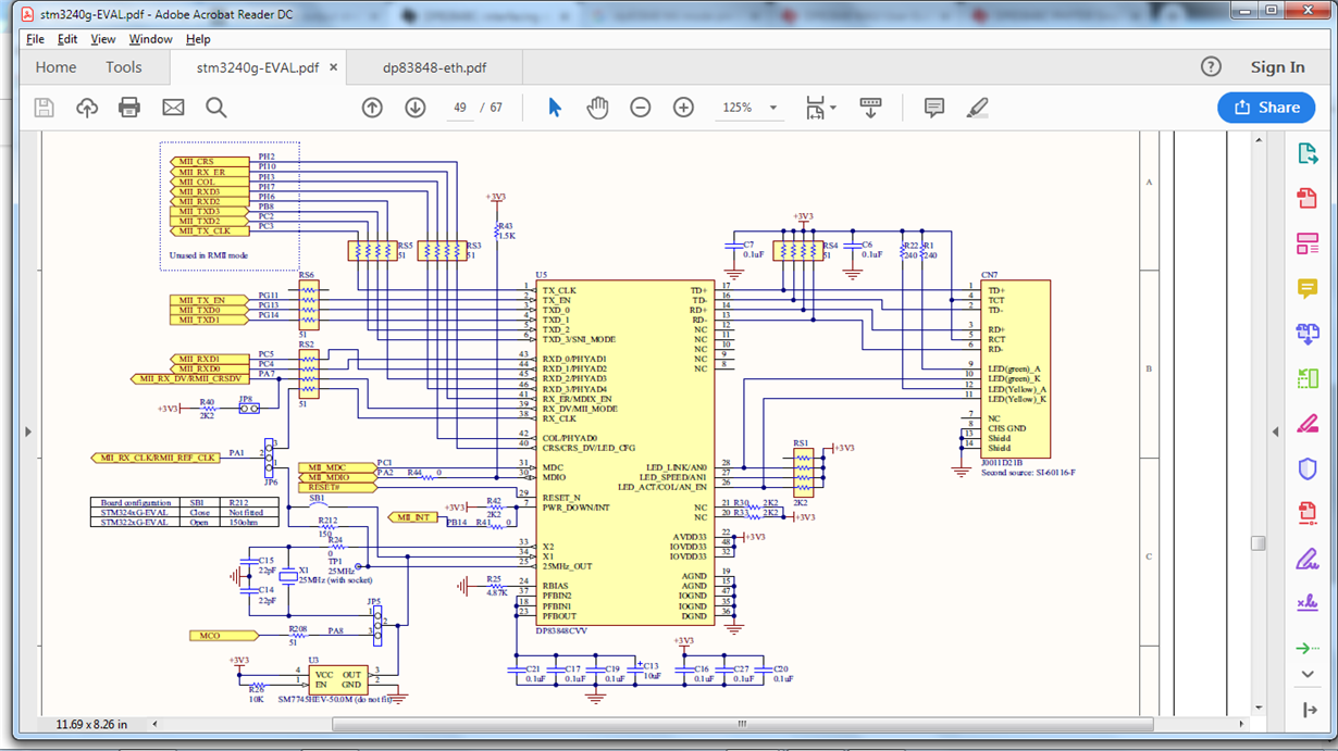
    the following image is the schematics of my connection the STM3240G-EVAL.

    Best Regards,

    siva

  • Hi Siva,

    Thank you for the schematic and code.

    How is the reference clock configured? Do you have an indication of how the jumpers JP5, JP6, and the selection resistors R212, and R26 are present or not?

    I'd also like to see your register values from 0x0 to 0x9.

    Best Regards,
  • Hi Rob Rodrigues,

    In JP6 jumper 2 and 3 is selected to enable MII interface mode
    In JP5 jumper 2 and 3 is selected to provide 25MHz clock for MII by MCO at PA8

    R212 resistor is not present
    R26 resistor is present but U3 is not fitted

    Which register values from 0x0 to 0x09 to be read??

    Best Regards,

    Siva

  • Siva,

    And is X1 populated in its socket? Can you measure the frequency of X1 pin to ensure the 25MHz reference is there and within +/50 ppm of 25MHz?

    I would like you to read the MDIO registers inside of the PHY and give me the values. From address 0x00 to 0x09

    Best,