This thread has been locked.

If you have a related question, please click the "Ask a related question" button in the top right corner. The newly created question will be automatically linked to this question.

TPD1S514: Routing

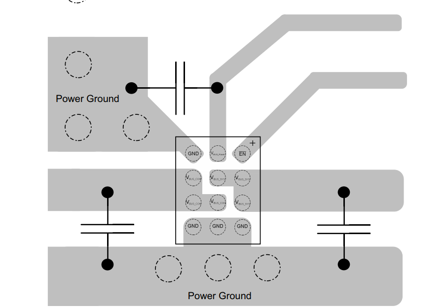
Part Number: TPD1S514

In the data sheet it states :-

When designing layout for the TPD1S514 Family, note that VBUS_CON and VBUS_SYS pins allow extra wide traces for
good power delivery. In the example shown, these pins are routed with 50 mil (1.27 mm) wide traces. Place the
VBUS_CON, VBUS_SYS, and VBUS_POWER capacitors as close to the pins as possible.

The pin separation is only 0.4mm so how could it be possible to get a 1.27mm(50 mil) track ?

The max Track width that I could get was 0.66mm(26 mil) !!??

  • The Layout Example in section 11.2 shows the best practice layout.  The Each of the 3 high power paths VBUS_CON VBUS_SYS and GND all have a 1.27mm main track route in this case, but they do neck down to connect to the internal balls.  The corner ground connection is also small, but this connection is no the high current path, so it will not impact performance.

     1

  • Thank you for your reply.

    It would be great if the data sheet could be updated to make these details more obvious.

    "but they do neck down to connect to the internal balls" wouldn't this lead to a bottle neck for the current and then wouldn't the 1.27mm track be irrelevant ?

  • The main current path is to the two external balls which will fully benefit from the wider route and the inner ball allows for the best possible current conduction path into the part. The third inner ball does play a significant role in the total current conduction path as well.

    The layout shown in the datasheet is the layout that is used on our EVM and characterization boards to get the maximum performance from the part.