This thread has been locked.

If you have a related question, please click the "Ask a related question" button in the top right corner. The newly created question will be automatically linked to this question.

TLK10232: Problem with registers value

Part Number: TLK10232

Hi,

For a new project, i use a TLK10232 for 10Gb link.

The high speed side need to comunicate at  10.312Gb and Low speed at 3.125Gb.

In my schematic :

1/ MODE_SEL = ST = '0'  (pull down 4.7K) for 10GBASE-KR mode.

2/ Refclk0 = refclk1 = 156.25MHz (refclk1 is only present in case of future problem but only refclk0 will be used).

3/ All channel A & B will be used at the same frame rate HS & LS side.

I developed a communication interface with MDIO.This interface works well. I can read or write all registers but i have 3 problems. The 3 problems appear on CHANNEL A and B.

In my software application, il only pass PDTRXA_N and  PDTRXB_N  to high level (initialized at low level) . And after i read all registers (without any initialization or modification before).

All values can be see in XAUI_MDIO_REGISTER_CHANNELA2.txt 


######################################################################################
######################    Vendor Specific Device Registers    ########################
######################################################################################
REGISTER GLOBAL_CONTROL_1		: 0x610

	REGISTER CHANNEL_CONTROL_1		: 0xb24 (need 0x0b00) ti use only

REGISTER HS_SERDES_CONTROL_1		: 0x831d
REGISTER HS_SERDES_CONTROL_2		: 0xa848
REGISTER HS_SERDES_CONTROL_3		: 0x1500
REGISTER HS_SERDES_CONTROL_4		: 0x2000
REGISTER LS_SERDES_CONTROL_1		: 0xf115

	REGISTER LS_SERDES_CONTROL_2		: 0x0 (need 0xDC04)
	REGISTER LS_SERDES_CONTROL_3		: 0x0 (need 0x000d) ti use only

REGISTER HS_OVERLAY_CONTROL		: 0x380
REGISTER LS_OVERLAY_CONTROL		: 0x4000
REGISTER LOOPBACK_TP_CONTROL		: 0xd10

	REGISTER LS_CONFIG_CONTROL		: 0x371 (need 0x0330) ti use only

REGISTER CLK_CONTROL			: 0x2f80
REGISTER RESET_CONTROL			: 0x0

	REGISTER CHANNEL_STATUS_1		: 0x2000 (need 0x0000) loss of signal indicator @ '1'

REGISTER HS_ERROR_COUNTER		: 0xfffd
REGISTER LS_LN0_ERROR_COUNTER		: 0xfffd
REGISTER LS_LN1_ERROR_COUNTER		: 0xfffd
REGISTER LS_LN2_ERROR_COUNTER		: 0xfffd
REGISTER LS_LN3_ERROR_COUNTER		: 0xfffd

	REGISTER LS_STATUS_1			: 0x8404 (need 0x0000) LS Invalid decode error for selected lane.
	REGISTER HS_STATUS_1			: 0xc000 (need 0x0000) ti use only

REGISTER DST_CONTROL_1			: 0x2000
REGISTER DST_CONTROL_2			: 0xc20
REGISTER DSR_CONTROL_1			: 0x2500
REGISTER DSR_CONTROL_2			: 0x4c20

	REGISTER DATA_SWITCH_STATUS		: 0x0 (need 0x1020) no coherent bit 15

REGISTER LS_CH_CONTROL_1		: 0x0
REGISTER HS_CH_CONTROL_1		: 0x0
REGISTER EXT_ADDRESS_CONTROL		: 0x0
REGISTER EXT_ADDRESS_DATA		: 0x0
REGISTER VS_10G_LN_ALIGN_ACODE_P	: 0x283
REGISTER VS_10G_LN_ALIGN_ACODE_N	: 0x17c
REGISTER MC_AUTO_CONTROL		: 0xf
REGISTER DST_ON_CHAR_CONTROL		: 0x2fd
REGISTER DST_OFF_CHAR_CONTROL		: 0x2fd
REGISTER DST_STUFF_CHAR_CONTROL		: 0x207
REGISTER DSR_ON_CHAR_CONTROL		: 0x2fd
REGISTER DSR_OFF_CHAR_CONTROL		: 0x2fd
REGISTER DSR_STUFF_CHAR_CONTROL		: 0x207
REGISTER LATENCY_MEASURE_CONTROL	: 0x0
REGISTER LATENCY_COUNTER_2		: 0x0
REGISTER LATENCY_COUNTER_1		: 0x0
REGISTER TRIGGER_LOAD_CONTROL		: 0x0
REGISTER TRIGGER_EN_CONTROL		: 0x0

######################################################################################
###########################    PMA/PMD Registers    ##################################
######################################################################################
REGISTER PMA_CONTROL_1			: 0x0
REGISTER PMA_STATUS_1			: 0x2
REGISTER PMA_DEV_IDENTIFIER_1		: 0x4000
REGISTER PMA_DEV_IDENTIFIER_2		: 0x5100
REGISTER PMA_SPEED_ABILITY		: 0x11
REGISTER PMA_DEV_PACKAGE_1		: 0xb
REGISTER PMA_DEV_PACKAGE_2		: 0x4000
REGISTER PMA_STATUS_2			: 0xb000
REGISTER PMA_RX_SIGNAL_DET_STATUS	: 0x0
REGISTER PMA_EXTENDED_ABILITY		: 0x50
REGISTER LT_TRAIN_CONTROL		: 0x2
REGISTER LT_TRAIN_STATUS		: 0x0
REGISTER LT_LINK_PARTNER_CONTROL	: 0x0
REGISTER LT_LINK_PARTNER_STATUS		: 0x0
REGISTER LT_LOCAL_DEVICE_CONTROL	: 0x0
REGISTER LT_LOCAL_DEVICE_STATUS		: 0x0
REGISTER KX_STATUS			: 0x3000
REGISTER KR_FEC_ABILITY			: 0x3
REGISTER KR_FEC_CONTROL			: 0x0
REGISTER KR_FEC_C_COUNT_1		: 0x0
REGISTER KR_FEC_C_COUNT_2		: 0x0
REGISTER KR_FEC_UC_COUNT_1		: 0x0
REGISTER KR_FEC_UC_COUNT_2		: 0x0
REGISTER KR_VS_FIFO_CONTROL_1		: 0xcc4c
REGISTER KR_VS_TP_GEN_CONTROL		: 0x0
REGISTER KR_VS_TP_VER_CONTROL		: 0x0
REGISTER KR_VS_CTC_ERR_CODE_LN0		: 0xce00
REGISTER KR_VS_CTC_ERR_CODE_LN1		: 0x0
REGISTER KR_VS_CTC_ERR_CODE_LN2		: 0x0
REGISTER KR_VS_CTC_ERR_CODE_LN3		: 0x80
REGISTER KR_VS_LN0_EOP_ERROR_COUNTER	: 0xfffd
REGISTER KR_VS_LN1_EOP_ERROR_COUNTER	: 0xfffd
REGISTER KR_VS_LN2_EOP_ERROR_COUNTER	: 0xfffd
REGISTER KR_VS_LN3_EOP_ERROR_COUNTER	: 0xfffd
REGISTER KR_VS_TX_CTC_DROP_COUNT	: 0xfffd
REGISTER KR_VS_TX_CTC_INSERT_COUNT	: 0xfffd
REGISTER KR_VS_RX_CTC_DROP_COUNT	: 0xfffd
REGISTER KR_VS_RX_CTC_INSERT_COUNT	: 0xfffd
REGISTER KR_VS_STATUS_1			: 0x0

	REGISTER KR_VS_TX_CRCJ_ERR_COUNT_1	: 0xffff (need 0xfffd) error
	REGISTER KR_VS_TX_CRCJ_ERR_COUNT_2	: 0xffff (need 0xfffd) error
	REGISTER KR_VS_TX_LN0_HLM_ERR_COUNT	: 0xffff (need 0xfffd) error
	REGISTER KR_VS_TX_LN1_HLM_ERR_COUNT	: 0xffff (need 0xfffd) error
	REGISTER KR_VS_TX_LN2_HLM_ERR_COUNT	: 0xffff (need 0xfffd) error
	REGISTER KR_VS_TX_LN3_HLM_ERR_COUNT	: 0xffff (need 0xfffd) error
	REGISTER LT_VS_CONTROL_2		: 0x200 (need 0x0000) ti use only

######################################################################################
#############################       PCS Registers      ###############################
######################################################################################
REGISTER PCS_CONTROL			: 0x0
REGISTER PCS_STATUS_1			: 0x2
REGISTER PCS_STATUS_2			: 0x8001
REGISTER KR_PCS_STATUS_1		: 0x4
REGISTER KR_PCS_STATUS_2		: 0x0
REGISTER PCS_TP_SEED_A0			: 0x0
REGISTER PCS_TP_SEED_A1			: 0x0
REGISTER PCS_TP_SEED_A2			: 0x0
REGISTER PCS_TP_SEED_A3			: 0x0
REGISTER PCS_TP_SEED_B0			: 0x0
REGISTER PCS_TP_SEED_B1			: 0x0
REGISTER PCS_TP_SEED_B2			: 0x0
REGISTER CS_TP_SEED_B3			: 0x0
REGISTER PCS_TP_CONTROL			: 0x0
REGISTER PCS_TP_ERR_COUNT		: 0x0
REGISTER PCS_VS_CONTROL			: 0xb0
REGISTER PCS_VS_STATUS			: 0xfd

######################################################################################
#######################    Auto-Negotiation Registers  ###############################
######################################################################################
REGISTER AN_CONTROL			: 0x3000
REGISTER AN_STATUS			: 0x88
REGISTER AN_DEV_PACKAGE			: 0x80
REGISTER AN_ADVERTISEMENT_1		: 0x1001
REGISTER AN_ADVERTISEMENT_2		: 0x80
REGISTER AN_ADVERTISEMENT_3		: 0x4000
REGISTER AN_LP_ADVERTISEMENT_1		: 0x1
REGISTER AN_LP_ADVERTISEMENT_2		: 0x0
REGISTER AN_LP_ADVERTISEMENT_3		: 0x0
REGISTER AN_XNP_TRANSMIT_1		: 0x2000
REGISTER AN_XNP_TRANSMIT_2		: 0x0
REGISTER AN_XNP_TRANSMIT_3		: 0x0
REGISTER AN_LP_XNP_ABILITY_1		: 0x0
REGISTER AN_LP_XNP_ABILITY_2		: 0x0
REGISTER AN_LP_XNP_ABILITY_3		: 0x0
REGISTER AN_BP_STATUS			: 0x1
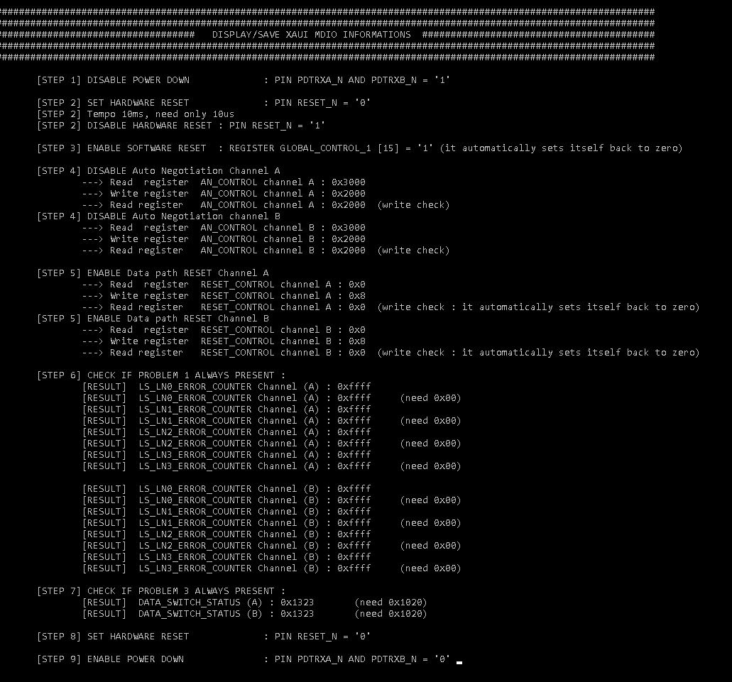
PROBLEM 1 : 

Some COR (Clear-On-Read) Register never pass to '0' when I read it.

For example LS_LN0_ERROR_COUNTERLS_LN1_ERROR_COUNTERLS_LN2_ERROR_COUNTER and LS_LN3_ERROR_COUNTER.

I don't try to test all COR Registers but these 4 registers never pass to 0 when i read it. I saw this problem when i tried to use test pattern.

Each time i read it value = default register = 0xFFFD.

PROBLEM 2 : 

It's the biggest problem because i cannot use LS side.

Register LS_SERDES_CONTROL_2 always equal to 0. I tried to write this register to default value 0xDC04 but when i read it again, value = 0.

I cannot change this register. In datasheet we can read that this register depend on PD_TRXx_N and LS_TX_ENRX register bit 1E.0001 bit 15.

In my configuration PD_TRXx_N = '1' (hardware check) and  LS_TX_ENRX register bit 1E.0001 bit 15 = '0' (Can be checked in .txt file).

PROBLEM 3 :  .

DATA_SWITCH_STATUS value = 0.  Default value is 0x1020. 

Here it's impossible to have bit [15:12] = 0000 because it's not a possible value in datasheet. It's Read Only register so i cannot try to fixe this value.

If someone can help me?

Thanks.

  • aitachour farid,

    I am looking into your issues and will get back to you as soon as possible.
  • aitachour farid,

    Sorry for the late reply. Please make sure you are following sections 7.6 and 7.7  of the TLK10232 datasheet for Clause 45 MDIO communication. Have you added a preamble to the MDIO communication? If not I suggest adding a 33bit of 1's for preamble in the MDIO communication, this may help with your issue. Also please ensure that you are following the MDIO frame format is as follows:

    ST /OP / PHYADDR / DEVTYPE / TA / (ADDR/DATA)  16BITS

  • Hi Malik Barton,

    I use a preamble. Before the post i used 32 Bits but now i change the value to 64 (in the goal to be sure) and problem is already present.

    I also decrease frequency  of MDC pin (from 10MHz to approximately 600KHz). It's the same things.

    For informations, i only use clause 45 with 3 differents frame :

    FRAME 1 :  Figure 7-5. CL45 - Management Interface Extended Space Address Timing

    FRAME 2 :  Figure 7-6. CL45 - Management Interface Extended Space Write Timing

    FRAME 3 :  Figure 7-7. CL45 - Management Interface Extended Space Read Timing

    When a communication appears, i always fixe the address with FRAME1 and after FRAME 2 or  3 depend on a write or read access. A preamble is always send before each frame.

    I had also check the frame format and for me it's good.

    ST = "00"

    OP = "00"  for address access, "01" for write access and  "11"  for read access

    PHYADR = "00000" for channel A and "00001" for channel B (in schematic PRTAD[0:4] = 00000).

    DEV_ADDR = x"1E" or x"01" or x"03" or x07"

    TA = "10" for write address or write access and "Z0" for read access.

    I don't think it's a trame problem because i only have problems with specific registers (focus principaly on LOW SPEED side).

    I can read register several time, result is always the same. 

    I can place temporisation or write before, result will be the same. 

    Is it possible that a harware problem cause register problem?

    jtag pin is not connected, except tck to gnd. TESTEN and GPIO pins are connected to gne with a 4.7Kohms resistor.


    Thanks. 

  • Ok i found the solution of problem N°2 :

    Register LS_SERDES_CONTROL_2 always equal to 0. I tried to write this register to default value 0xDC04 but when i read it again, value = 0.
    I cannot change this register. In datasheet we can read that this register depend on PD_TRXx_N and LS_TX_ENRX register bit 1E.0001 bit 15.
    In my configuration PD_TRXx_N = '1' (hardware check) and LS_TX_ENRX register bit 1E.0001 bit 15 = '0' (Can be checked in .txt file).

    The problem is on register LS_SERDES_CONTROL_1 bit 15:12 (LS_LN_CFG_EN[3:0])

    Read values in LS_SERDES_CONTROL_2 and LS_SERDES_CONTROL_3 and LS_CH_CONTROL_1 reflect the settings value for Lane selected through LS_LN_CFG_EN[3:0].
    But LS_LN_CFG_EN[3:0] = 1111 by default. It's not a possible value (similar to read register value of lane 0, 1 , 2 and 3 in the same register).

    If i use LS_LN_CFG_EN[3:0] = 0001 (To read Lane 0 settings,) , the value of register LS_SERDES_CONTROL_2 is 0xDC04 (default value) and not 0000.


    Nevertheless, problem N°1 et 3 are always presents. If someone can help me :


    PROBLEM 1 :
    Some COR (Clear-On-Read) Register never pass to '0' when I read it.
    For example LS_LN0_ERROR_COUNTER, LS_LN1_ERROR_COUNTER, LS_LN2_ERROR_COUNTER and LS_LN3_ERROR_COUNTER.
    I don't try to test all COR Registers but these 4 registers never pass to 0 when i read it. I saw this problem when i tried to use test pattern.
    Each time i read it value = default register = 0xFFFD.


    PROBLEM 3 : .
    DATA_SWITCH_STATUS value = 0. Default value is 0x1020.
  • aitachour farid,

    I am still looking into your issue but have not found a complete solution as of yet. I will update you when I have something more concrete for your remaining issues. 

  • Can you reproduce the 2 problems?

    Please can you give me all access that your "TLK10232 EVM GUI Software" send to the TLK10232?

    If you don't have these problems with  your TLK10232 EVM GUI Software , it's perahps because we need to initialize some registers before.

    Thanks.
  • Hi,

    Any update?

    Regards,
  • aitachour farid,

    Unfortunately I have not been able to reproduce problem 1 and 3 with the EVM GUI nor can I find any issues in the EVM code. I have not been able to find any previous issues reported with the GUI either. I am currently checking to see if i can give you "full access" but I do not think this is likely. I am still pursing solutions. Just to confirm you are using the EVM with the USB Dongle Board? Or are you using an external MDIO data controller?

  • aitachour farid,

    Is there any more support needed for this issue? If so please reply with any relevant details so that I can further assist you. For now I will be marking this thread as "TI Thinks Resolved". If you have resolved your issue, please post the solution to the original problem/post for others with similar issues.
  • I use external MDIO data controller and not EVM with the USB Dongle Board.

    Problem 2 is the proof that we cannot read the default value noted in the datasheet just after a reset of the component.
    So it's impossible that your EVM GUI only reset component and after can read the value of the datasheet.
    It's necessary to modify some registers before.
    I just need the list and value of these register.
    I don't want the complete code of the EVM GUI , but only register acces that the EVM GUI do after reset.

    If it's not possible, so change and update the datasheet.
  • So any update?

    I'm waiting for more that 1 month now without any useful response that can help me ...
  • aitachour farid,

    Have you tried to execute a data path reset after de-asserting PD_TRXx_N using register RESET_CONTROL bit 3 before reading all registers? The is required once the desired functional mode is configured.

    Another potential solution to Problem 1 and 3 could be that the part is in Auto Negotiation mode directly after power up. Please try to disable Auto Negotiation (AN) by using the AN_ENABLE bit field. After disabling Auto Negotiation please issue a data path reset. AN is on by default and cause the internal data switch not to report its status until AN is completed. This could also affect the LS Error Counters.

    My apologies for the delay in the answering this issue. There were many delays in finding design files that could help find a solution to this issue.  

  • Malik Barton57,

    You can find all access and result of the test.

    Up to now, i always reseted the component with a hardware reset. I add a software reset in step 3, but normally it change nothing.

    When i disable Auto Negotiation, results change but problems are always here.

    For problem N°1 : 

    Before Auto Negotiation modification, i had all LS_COUNTER initiated to 0xFFFD (correct value) but register never pass to 0 after a read.

    Now, All LS_COUNTER are initiated @ 0xFFFF (no correct value) and register value never pass to 0 (can be see in step 6 ).

    For problem N°3 (step 7) :

    Before Auto Negotiation modification, DATA_SWITCH_STATUS register was = 0  (correct value 0x1020).

    Now DATA_SWITCH_STATUS register = 0x1323.  Seem to be better but it's not the correct value.  Differences seem to be about "ON / OFF condition indicator" but they don't have any information about that in datasheet.

  • aitachour farid,

    Are you applying a appropriate signal to the REFCLK pin when running this test? I would like to make sure that HS and LS PLL are locked before you try to read the COR registers? Could you provide a updated register dump after this test where HS_PLL_LOCK and LS_PLL_LOCK are 1? If you are having issues getting the PLL to lock please make sure the input reference clock is at the expected frequency and has low jitter. Also could you read other COR registers and LL/LH bit fields such as HS_ERROR_COUNTER and KX_STATUS to see if you are having similar issues?
  • Hi,

    The problem N°3 is resolved. DATA_SWITCH_STATUS Register have RO/LH bit so we need to read two times the register.

    Now only problem 2 is present (cor register never read as null).

    About your questions : 

    PLL are locked (read two times register CHANNEL_STATUS_1 : see result in attachment step 6).

    Problem only appear in LS_LNx_ERROR_COUNTER.

    Problem don't appear on Register HS_ERROR_COUNTER and KX_STATUS (step 9 in picture in attachment).

    I send (in attachment) the value of all register in the .txt file.

    
    #####################################################################################################################
    ####################################    Vendor Specific Device Registers    #########################################
    #####################################################################################################################
    REGISTER GLOBAL_CONTROL_1		: 0x610
    REGISTER CHANNEL_CONTROL_1		: 0xb24
    REGISTER HS_SERDES_CONTROL_1		: 0x831d
    REGISTER HS_SERDES_CONTROL_2		: 0xa848
    REGISTER HS_SERDES_CONTROL_3		: 0x1500
    REGISTER HS_SERDES_CONTROL_4		: 0x2000
    REGISTER LS_SERDES_CONTROL_1		: 0xf115
    REGISTER LS_SERDES_CONTROL_2		: 0x0
    REGISTER LS_SERDES_CONTROL_3		: 0x0
    REGISTER HS_OVERLAY_CONTROL		: 0x380
    REGISTER LS_OVERLAY_CONTROL		: 0x4000
    REGISTER LOOPBACK_TP_CONTROL		: 0xd10
    REGISTER LS_CONFIG_CONTROL		: 0x371
    REGISTER CLK_CONTROL			: 0x2f80
    REGISTER RESET_CONTROL			: 0x0
    REGISTER CHANNEL_STATUS_1		: 0x1003
    REGISTER HS_ERROR_COUNTER		: 0x0
    REGISTER LS_LN0_ERROR_COUNTER		: 0xffff
    REGISTER LS_LN1_ERROR_COUNTER		: 0xffff
    REGISTER LS_LN2_ERROR_COUNTER		: 0xffff
    REGISTER LS_LN3_ERROR_COUNTER		: 0xffff
    REGISTER LS_STATUS_1			: 0x8c16
    REGISTER HS_STATUS_1			: 0xf03c
    REGISTER DST_CONTROL_1			: 0x2000
    REGISTER DST_CONTROL_2			: 0xc20
    REGISTER DSR_CONTROL_1			: 0x2500
    REGISTER DSR_CONTROL_2			: 0x4c20
    REGISTER DATA_SWITCH_STATUS		: 0x1023
    REGISTER LS_CH_CONTROL_1		: 0x0
    REGISTER HS_CH_CONTROL_1		: 0x0
    REGISTER EXT_ADDRESS_CONTROL		: 0x0
    REGISTER EXT_ADDRESS_DATA		: 0x0
    REGISTER VS_10G_LN_ALIGN_ACODE_P	: 0x283
    REGISTER VS_10G_LN_ALIGN_ACODE_N	: 0x17c
    REGISTER MC_AUTO_CONTROL		: 0xf
    REGISTER DST_ON_CHAR_CONTROL		: 0x2fd
    REGISTER DST_OFF_CHAR_CONTROL		: 0x2fd
    REGISTER DST_STUFF_CHAR_CONTROL		: 0x207
    REGISTER DSR_ON_CHAR_CONTROL		: 0x2fd
    REGISTER DSR_OFF_CHAR_CONTROL		: 0x2fd
    REGISTER DSR_STUFF_CHAR_CONTROL		: 0x207
    REGISTER LATENCY_MEASURE_CONTROL	: 0x0
    REGISTER LATENCY_COUNTER_2		: 0x0
    REGISTER LATENCY_COUNTER_1		: 0x0
    REGISTER TRIGGER_LOAD_CONTROL		: 0x0
    REGISTER TRIGGER_EN_CONTROL		: 0x0
    
    #####################################################################################################################
    ###########################################    PMA/PMD Registers    #################################################
    #####################################################################################################################
    REGISTER PMA_CONTROL_1			: 0x0
    REGISTER PMA_STATUS_1			: 0x82
    REGISTER PMA_DEV_IDENTIFIER_1		: 0x4000
    REGISTER PMA_DEV_IDENTIFIER_2		: 0x5100
    REGISTER PMA_SPEED_ABILITY		: 0x11
    REGISTER PMA_DEV_PACKAGE_1		: 0xb
    REGISTER PMA_DEV_PACKAGE_2		: 0x4000
    REGISTER PMA_STATUS_2			: 0xb800
    REGISTER PMA_RX_SIGNAL_DET_STATUS	: 0x1
    REGISTER PMA_EXTENDED_ABILITY		: 0x50
    REGISTER LT_TRAIN_CONTROL		: 0x2
    REGISTER LT_TRAIN_STATUS		: 0x6
    REGISTER LT_LINK_PARTNER_CONTROL	: 0x0
    REGISTER LT_LINK_PARTNER_STATUS		: 0x0
    REGISTER LT_LOCAL_DEVICE_CONTROL	: 0x2
    REGISTER LT_LOCAL_DEVICE_STATUS		: 0x0
    REGISTER KX_STATUS			: 0x3001
    REGISTER KR_FEC_ABILITY			: 0x3
    REGISTER KR_FEC_CONTROL			: 0x0
    REGISTER KR_FEC_C_COUNT_1		: 0x0
    REGISTER KR_FEC_C_COUNT_2		: 0x0
    REGISTER KR_FEC_UC_COUNT_1		: 0x0
    REGISTER KR_FEC_UC_COUNT_2		: 0x0
    REGISTER KR_VS_FIFO_CONTROL_1		: 0xcc4c
    REGISTER KR_VS_TP_GEN_CONTROL		: 0x0
    REGISTER KR_VS_TP_VER_CONTROL		: 0x0
    REGISTER KR_VS_CTC_ERR_CODE_LN0		: 0xce00
    REGISTER KR_VS_CTC_ERR_CODE_LN1		: 0x0
    REGISTER KR_VS_CTC_ERR_CODE_LN2		: 0x0
    REGISTER KR_VS_CTC_ERR_CODE_LN3		: 0x80
    REGISTER KR_VS_LN0_EOP_ERROR_COUNTER	: 0x0
    REGISTER KR_VS_LN1_EOP_ERROR_COUNTER	: 0x0
    REGISTER KR_VS_LN2_EOP_ERROR_COUNTER	: 0x0
    REGISTER KR_VS_LN3_EOP_ERROR_COUNTER	: 0x0
    REGISTER KR_VS_TX_CTC_DROP_COUNT	: 0x0
    REGISTER KR_VS_TX_CTC_INSERT_COUNT	: 0x0
    REGISTER KR_VS_RX_CTC_DROP_COUNT	: 0x0
    REGISTER KR_VS_RX_CTC_INSERT_COUNT	: 0x25b
    REGISTER KR_VS_STATUS_1			: 0x0
    REGISTER KR_VS_TX_CRCJ_ERR_COUNT_1	: 0xffff
    REGISTER KR_VS_TX_CRCJ_ERR_COUNT_2	: 0xffff
    REGISTER KR_VS_TX_LN0_HLM_ERR_COUNT	: 0xffff
    REGISTER KR_VS_TX_LN1_HLM_ERR_COUNT	: 0xffff
    REGISTER KR_VS_TX_LN2_HLM_ERR_COUNT	: 0xffff
    REGISTER KR_VS_TX_LN3_HLM_ERR_COUNT	: 0xffff
    REGISTER LT_VS_CONTROL_2		: 0x200
    
    #####################################################################################################################
    ###########################################      PCS Registers      #################################################
    #####################################################################################################################
    REGISTER PCS_CONTROL			: 0x0
    REGISTER PCS_STATUS_1			: 0x82
    REGISTER PCS_STATUS_2			: 0x8c01
    REGISTER KR_PCS_STATUS_1		: 0x4
    REGISTER KR_PCS_STATUS_2		: 0x0
    REGISTER PCS_TP_SEED_A0			: 0x0
    REGISTER PCS_TP_SEED_A1			: 0x0
    REGISTER PCS_TP_SEED_A2			: 0x0
    REGISTER PCS_TP_SEED_A3			: 0x0
    REGISTER PCS_TP_SEED_B0			: 0x0
    REGISTER PCS_TP_SEED_B1			: 0x0
    REGISTER PCS_TP_SEED_B2			: 0x0
    REGISTER CS_TP_SEED_B3			: 0x0
    REGISTER PCS_TP_CONTROL			: 0x0
    REGISTER PCS_TP_ERR_COUNT		: 0x0
    REGISTER PCS_VS_CONTROL			: 0xb0
    REGISTER PCS_VS_STATUS			: 0x0
    
    #####################################################################################################################
    #######################################    Auto-Negotiation Registers    ############################################
    #####################################################################################################################
    REGISTER AN_CONTROL			: 0x2000
    REGISTER AN_STATUS			: 0x98
    REGISTER AN_DEV_PACKAGE			: 0x80
    REGISTER AN_ADVERTISEMENT_1		: 0x1001
    REGISTER AN_ADVERTISEMENT_2		: 0x80
    REGISTER AN_ADVERTISEMENT_3		: 0x4000
    REGISTER AN_LP_ADVERTISEMENT_1		: 0x1
    REGISTER AN_LP_ADVERTISEMENT_2		: 0x0
    REGISTER AN_LP_ADVERTISEMENT_3		: 0x0
    REGISTER AN_XNP_TRANSMIT_1		: 0x2000
    REGISTER AN_XNP_TRANSMIT_2		: 0x0
    REGISTER AN_XNP_TRANSMIT_3		: 0x0
    REGISTER AN_LP_XNP_ABILITY_1		: 0x0
    REGISTER AN_LP_XNP_ABILITY_2		: 0x0
    REGISTER AN_LP_XNP_ABILITY_3		: 0x0
    REGISTER AN_BP_STATUS			: 0x9

    Best regards.

  • aitachour farid,

    I am currently looking into some design files to understand why you may be seeing this error. I will get back to you as soon as possible. Also have you tried reading the COR registers twice to see if it is the same issue as problem N°3?
  • All registers are read twice in this test :
    CHANNEL_STATUS_1 (for lock), DATA_SWITCH_STATUS, KX_STATUS, HS_ERROR_COUNTER and LS_LNx_ERROR_COUNTER.
    Read twice for channel A and twice for channel B.
  • aitachour farid,

    After some digging it seems that the your LS error counter saturation, in your case, should be caused by a lack on valid connection on the LS side. In other words the error counter will show 0xFFFD after its initial value after power-up. Once auto negotiation configuration is complete or auto negotiation is disabled and there is no valid data present on the LS, the LS error counters will increment to 0xFFFF. Once at 0xFFFF the error counters will only stay at this value if LS connection is not established, reading the LS error counters will not reset them until a valid LS connection is made. This seems to be your case based on the LOS and Channel Sync indicators in the LS_STATUS_1 register. When you are testing your device is there valid data on the LS side as expected (i.e. IDLE patterns)? Is their a physical connection on LS side of TLK10232? If you do have a valid connection and are transmitting valid data, could you report LS_STATUS_1 value? Could you try consecutive reads of this register outside of your established initialization sequence? You should see different values as the register increments towards 0xFFFF. Other than this the LS error registers are not related to other registers and should only be related to data flowing into the LS side of TLK10232.
  • Hi,
    In my first post, problem was DEFAULT REGISTER VALUE (value without any configuration except a reset).
    In this case you said me that all parameters need to be configured in the goal to have a correct LS side communication.

    But if i change register we are not in default case. it is not coherent.

    So before this message, the LS side was configured in Loopback mode.
    Now, i did a lot of change.
    1/ I correctly configured the XAUI register for communication in LS side.
    2/ The LS side is connected to a FPGA which send 0xBC k28.5 charactere in continu.

    Problem seem to have disappeared but i need to do more test before to confirm.

  • Hi,

    Have you confirmed that your issues have been resolved?
  • Hi,

    Is there any more support needed for this issue? If so please reply with any relevant details so that I can further assist you. For now I will be marking this thread as "TI Thinks Resolved". If you have resolved your issue, please post the solution to the original problem/post for others with similar issues.
  • PROBLEM 1 :

    LS_LN0_ERROR_COUNTER, LS_LN1_ERROR_COUNTER, LS_LN2_ERROR_COUNTER and LS_LN3_ERROR_COUNTER are some (CLEAR-ON-READ) COR registers. But if the LS side is not functional, these registers are always at xFFFF. These CLEAR-ON-READ registers cannot pass to 0 after a read if default register value of all others registers are used because in this case the LS side is not functional.

    PROBLEM 2 :

    The problem is on register LS_SERDES_CONTROL_1 bit 15:12 (LS_LN_CFG_EN[3:0]).

    Read values in LS_SERDES_CONTROL_2 and LS_SERDES_CONTROL_3 and LS_CH_CONTROL_1 reflect the settings value for Lane selected through LS_LN_CFG_EN[3:0].

    But LS_LN_CFG_EN[3:0] = 1111 by default. It's not a possible value (similar to read register value of lane 0, 1 , 2 and 3 in the same register).

    If i use LS_LN_CFG_EN[3:0] = 0001 (To read Lane 0 settings,) , the value of register LS_SERDES_CONTROL_2 is 0xDC04 (default value) and not 0000.

    PROBLEM 3 :

    DATA_SWITCH_STATUS Register have RO/LH bit so we need to read two times the register.