Because of the Thanksgiving holiday in the U.S., TI E2E™ design support forum responses may be delayed from November 25 through December 2. Thank you for your patience.

This thread has been locked.

If you have a related question, please click the "Ask a related question" button in the top right corner. The newly created question will be automatically linked to this question.

DS125BR401A: OOB Signal Questions

Part Number: DS125BR401A
Other Parts Discussed in Thread: DS125BR401

Dear Team,

My customer has a detection issue when connecting to a specific SAS HDD.

And they found that OOB signal of input side is different from the output side.

So we would like to know the reason why OOB signal are not the same. Please help to comment.

Is there any register that can adjust the signal detection signal?

Please refer to below figure.

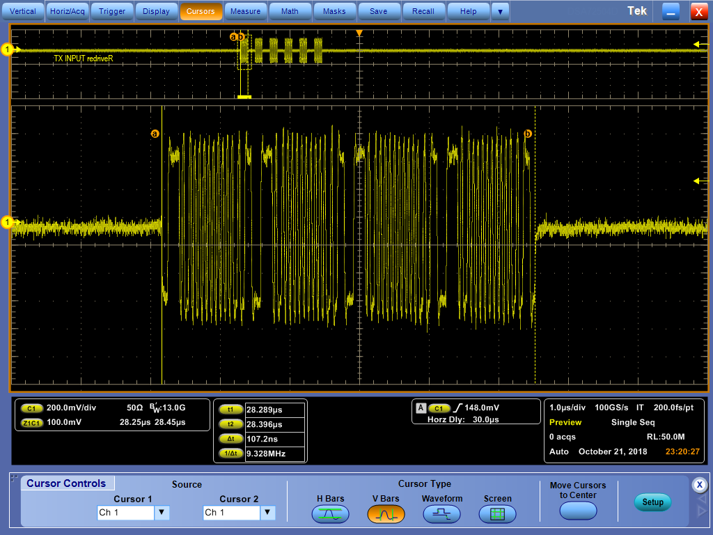
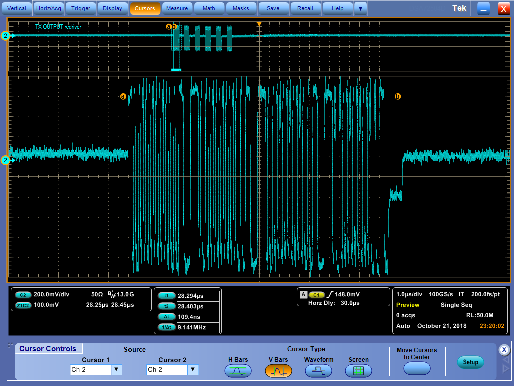
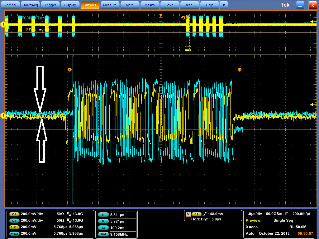
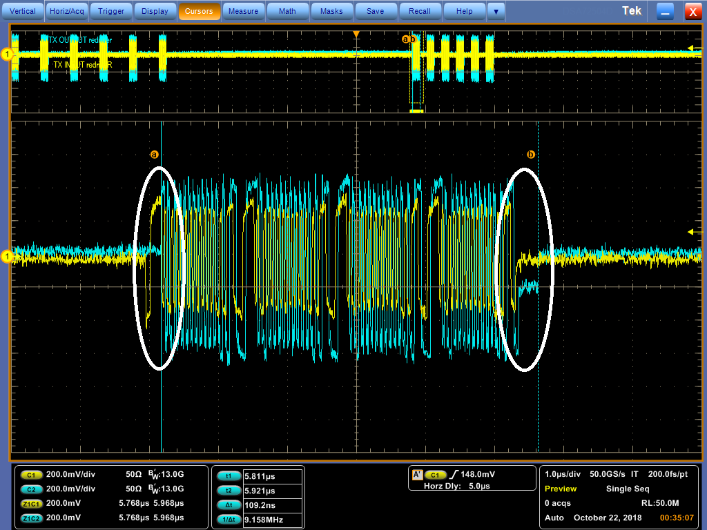
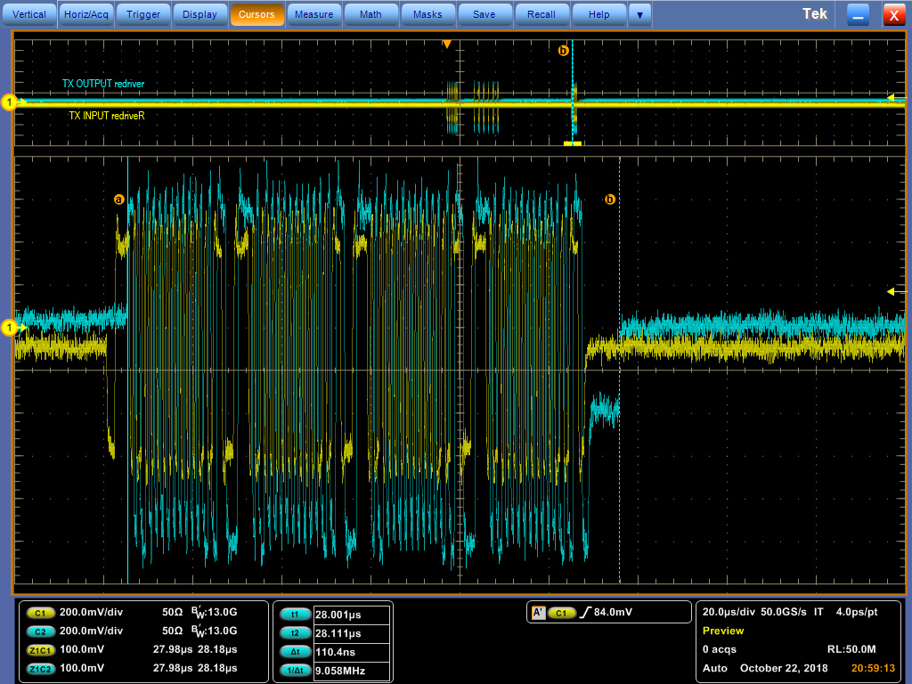
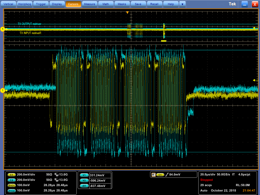
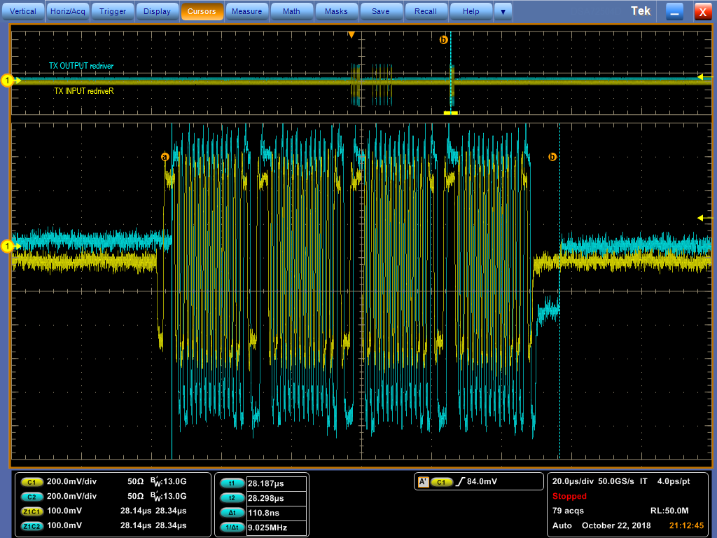
(Yellow Line is input signal, Blue Line is output signal)

Input OOB signal

Output OOB signal

Thank you.

  • Hi Jim,

    I thought Lee - one of my colleagues - has already responded to this question.

    If detection issue is due to OOB detection, then there are two control mechanism that could help. These are SD_TH and VOD. Please refer to the DS125BR401A data sheet to get more info regarding register settings and etc. You can sweep these two settings to change OOB level and timing.

    Regards,,nasser
  • Hi Jim and Nasser(sorry that I have no idea if Nasser is your name or not),

    Currently, we meet the SATA SSD cannot detecting issue and there are three question need your advise.

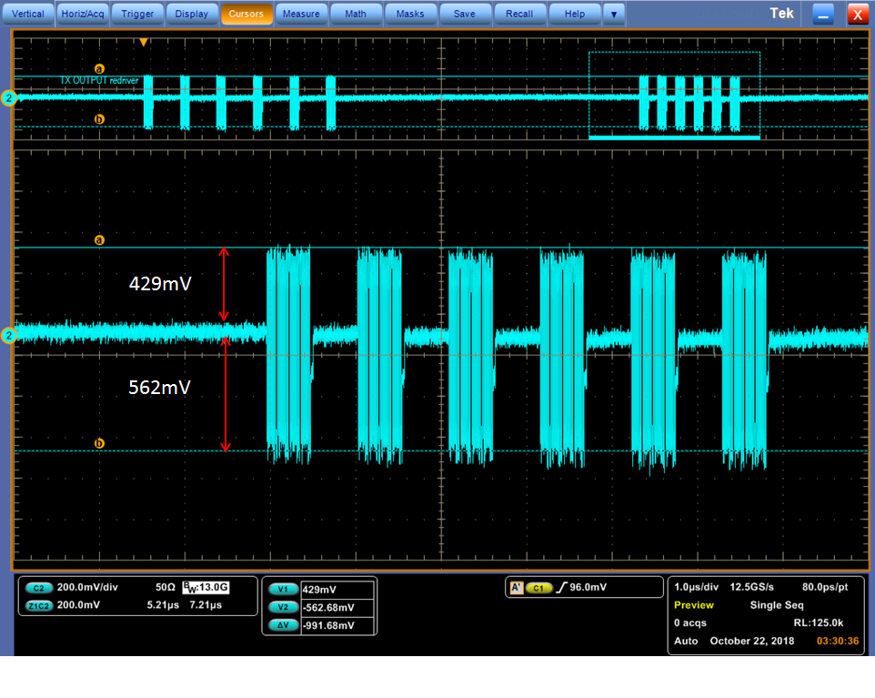
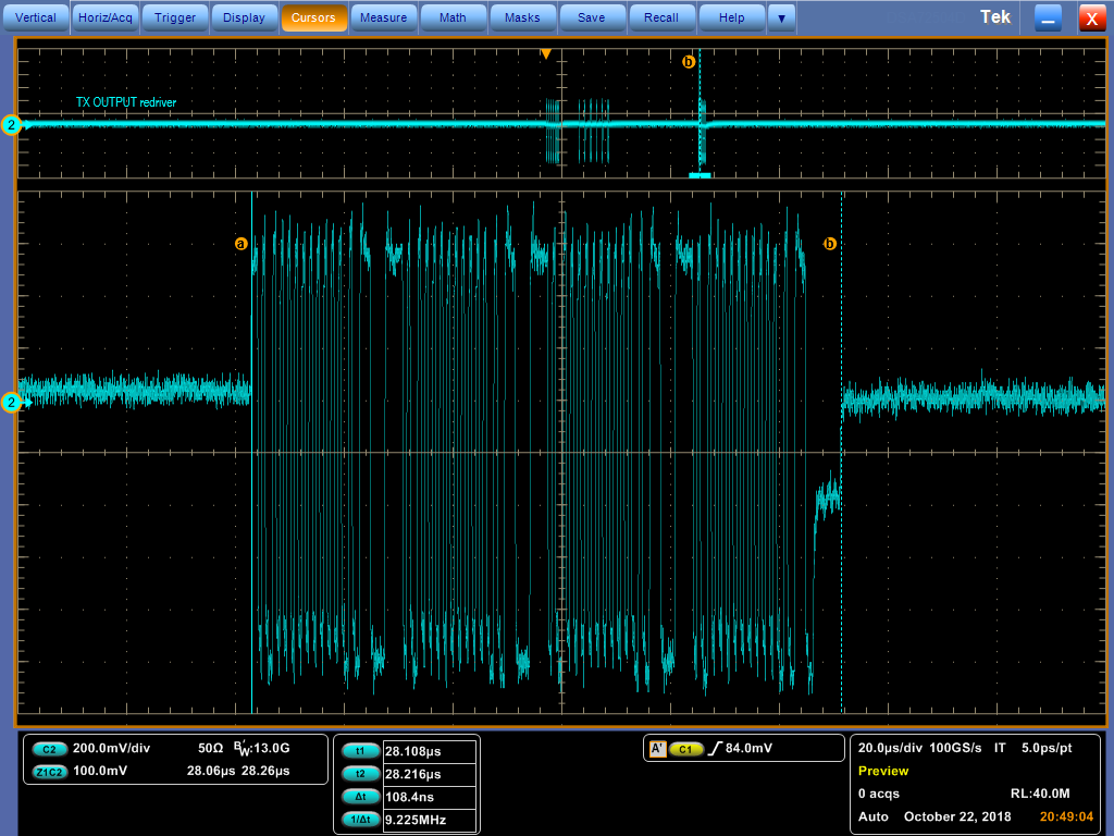
    1. The OOB signal 0 V lefel question:

       From the waveform1, we can see that the 0V of the output of waveform is not the same as original one.

       Yellow one is the Intel PCH SATA controller output signal and Blue one is hte output from DS123BR401A CH0 CHB

       Which register may related to this symptonm?

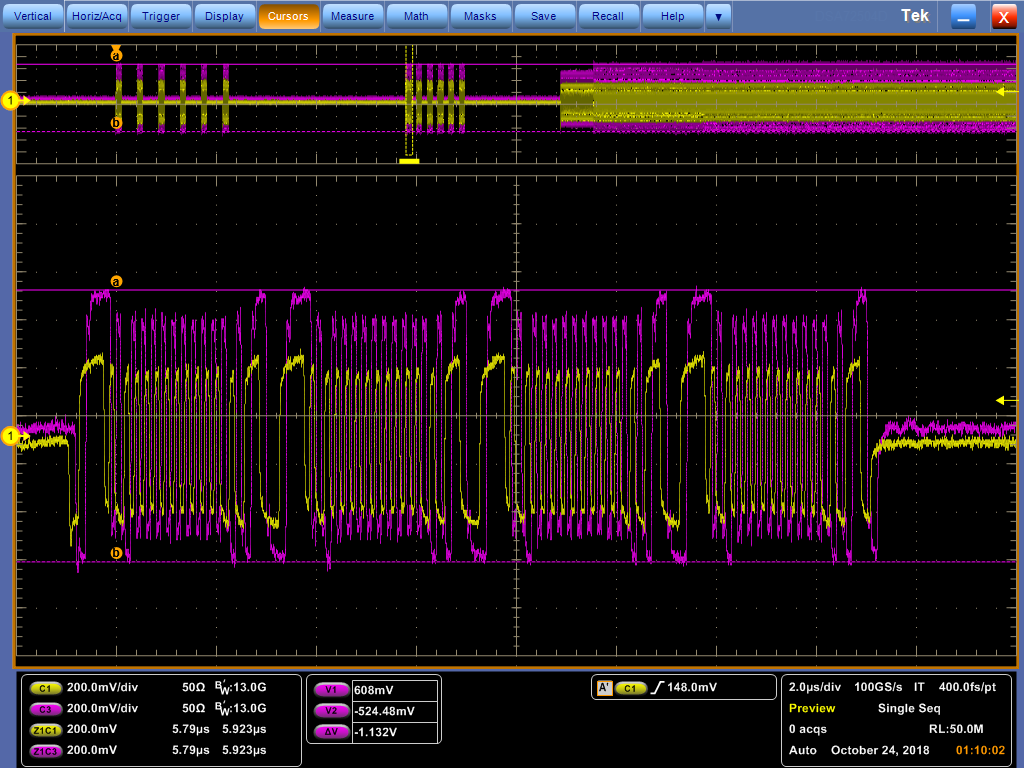
    2. The OOB output signal is not the "copy" of the original input one question:

        From the waveform2, the first low pulse from the PCH is not output by DS123BR401A and the end of the low pulse from the DS123BR401A does not go the 0 V, Could you advise which register can improve this situation?

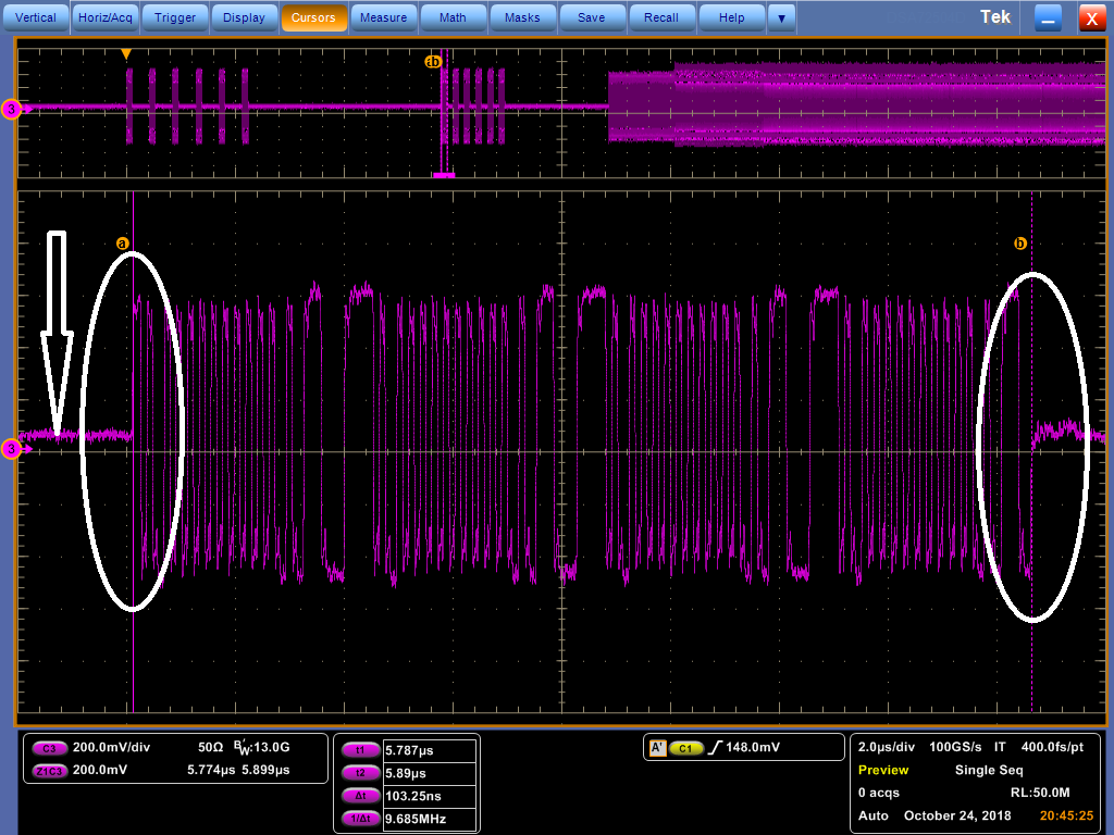
    3.  The OOB output from DS123BR401A does not symmetric question

       From Waveform3, we can see that the signal output from DS123BR401A is not symmetric, the high/low of the signal does not match and the delta are around 133mV. Base on your experience, could you please help to advise the register that can fix this symptom?

    Sorry that dye to the customer (Fujitsu Japan) is not request and asking to solve the issue, could you please feedback in detial?

    Tahnk you.

    Gary

  • Hi TI team,

    Here are some information of modification of SD_TH register.

    It seems the three question I mention is still no improvement.

    Please advise them.

    Thank you.

    Gary

     1. Set to 10 01 – Max. Assert threshold Min. De-assert threshold

    2. Set to 10 10 – Max. Assert threshold Max. De-assert threshold

    3. Set to 01 01 – Min. Assert threshold Min. De-assert threshold

    4.  Set to 01 10 – Min. Assert threshold Max. De-assert threshold

  • Hi TI Team,

    I update the latest information about this issue.

    After checking the issue before from TI Forums, I found that there are several reserved register that can help OOB signal.

    Write Channel B0 Register 0x0D[1] = 1’b (Force signal detect to always be “on” CH B0)
    Write Channel B1 Register 0x14[1] = 1’b (Force signal detect to always be “on” CH B1)
    Write Channel B2 Register 0x1B[1] = 1’b (Force signal detect to always be “on” CH B2)
    Write Channel B3 Register 0x22[1] = 1’b (Force signal detect to always be “on” CH B3)

    So I try about this and get good improvement on the OOB signal.

    But the 0V shift is still happened, it there any register or checkpoint to be recommanded?

    Any way, I still need TI's command about this register's function and explane it to customer.

    Thank you.

  • Hi Gary,

    The register bits listed do exactly as explained in previous posts.  They remove the Signal Detect circuit from the control path.  It is the signal detect circuit which was causing the delay you noticed in earlier waveform posts.  The output now responds immediately to the OOB signal input - eliminating this form of OOB distortion.

    There is an additional register which may help to minimize the DC offset you are observing between the input and the output.

    Write Register 0x4C = 01'h

    This disables a DC offset control loop.  This loop can be tricked by the "on" / "off" nature of the OOB signal resulting in a sub-optimal DC level. Disabling it results in better offset control in SATA applications.

    Regards

  • Hi Lee,
    Thanks for your explanation. It is quite clear.
    But I still have some question need your advise.
    1. for register 0x4C, 0x0D/14/1B change, is there any side effect to the normal SATA signal on the remove of Signal Detect circuit ? What should we pay attention if we apply this change?
    2. For the image builded from SigCon, we found that the EEPROM contents does not change if we use SigCon to change the register 0x4C, 0x0D/14/1B. It seems we do not have the premission to change the reserved register.
    Please advise us how to change the register in the EEPROM image.
    Thank you.
  • Hi Lee,

    I have one more question.

    3. Dose register 0x4C set to 01h works if we have already set 0x0D/14/1B to 02h?

    We have tried set 0x4C to 01h and found that it can solve the waveform2 end of signal, but not improvement the first signal.

    And also no help on waveform1 signal output 0V leve.

  • Gary,

    I recommend to write all of the registered discussed.  They work together to produce the best OOB waveform output.

    The input waveform (yellow) has a negative offset from 0V.  Could it just be the differential probe P/N is switched from one channel to the other?

    Regards,

    Lee

  • Changing register 0x4C in the EEPROM must be done manually by editting the file.

    The EEPROM data is defined in the datasheet with Table 9.  The attachment below is pulled from the table to show the location of register 0x4C[0].

    The bits in registers 0x0D/14/1B/22 are not in the EEPROM register map.

    I will investigate another method to do this with register bits which can be accessed via the EEPROM.

    Regards,

    Lee

  • Hi Lee,
    Thanks for the advise.
    Our Japan Customer find that the register do not have detail description about these register, so they request us to get more information from TI.

    1. What is the root cause of this non detection issue?
    Which spec item was violated and how it violated?

    2. Register changing: 0x0D/0x14/0x1B to 02h
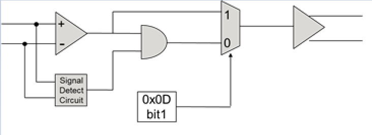
    (1) Would you provide diagram of this Signal Detect Circuit ? We want to know its implementation more.
    (2) Does this setting affect to only OOB? No affect to 6G SAS data?
    (3) With this setting, OOB burst pattern got better to symmetric with high and low voltage.
    Does this setting affect to a driver characteristics of output?

    3. Register changing: 0x4C to 01h
    (1) We need more detail description of this bit.
    (2) Would you provide diagram of this circuit ? We want to know its implementation more.
    (3) When input side has some offset, does it propagate to output side?
    (4) Does this setting affect to only OOB? No affect to 6G SAS data?

    4. Termination of input side
    Signals from controller to re-driver are AC coupling.
    In this case, DC offset is defined by input termination of re-driver, we think.
    Would you provide terminal circuit of re-driver.

    Thank you.
    Gary
  • 1. It looks like the root cause for failure is OOB Transmit Burst Timing.  In same waveforms it is over 110ns.  The specification maximum is 109.9ns.

    2. The signal detect circuit uses energy detection to determine if there is a valid signal present on the input or not.  As you saw in the waveforms, it takes a few nanoseconds for this circuit to function and turn-on or turn-off the repeater output. 

    2.2 This setting will only impact OOB transmission, the threshold is low so it will never turn-off when valid data is present.

    2.3 The improved OOB setting will not change the normal driver output.

    3. This bit is used to enable or disable DC offset correction for the internal signal path.  By default the register bit is enabled when the value = 0.  Writing a value of "1" disables this function. 

    3.2 This circuit was designed to adjust for wafer fabrication variation.  Now that this is a mature process we understand it is actually not needed.  I cannot discuss the specific implementation details. The offset correction circuit bandwidth and OOB signaling can combine to give poor offset correction result.  This is seen when the waveform is not balanced between the top and bottom amplitudes.

    3.3 Yes, this is a linear device when dealing with very small input voltages. If there is a differential offset on the input, it is very likely to show up on the output.

    4. The offset can still get though the system AC coupling.  Eventually the voltage will decay, but the time constant is longer than the OOB pulse timing. 

    The input termination network is 2x 50 ohms to VDD.

    Regards,

    Lee  

  • Hi Lee,
    Thanks for the update and I will check it with customer.
    BTW, please help to keep checking how to modify the 0x0D/0x14/0x1B in the EEPROM.
    Thank you.
  • Hi Lee,

    Customer inform more question that need your advise.

    Question from 1:

    My understanding is that gap length is more important than burst length to distinguish COMRESET, COMWAKE and COMSAS.

    Is it correct understanding for your explanation that both nominal length of burst and gap of COMWAKE are same and if burst length gets longer then gap length will be shorter, right?

    Question from 2:

     (4) Following block diagram shows my understanding. When we set 0x0D to 02h, data will propagates simply. When we set 0x0D to 00h detect circuit gate the signal, right?

     (5) I want to confirm about this sentence  “the threshold is low so it will never turn-off when valid data is present”.

         This circuit is always on when 6G data is valid. But it does not affect when we set 0x0D to 02h, right?

     (6) When we disable signal detect circuit, what is the demerit?

        I believe you have strong advantage with this circuit because default setting of this circuit is enable and no ROM mapping to disable.

        What is the advantage when we use this circuit and what is the disadvantage when we don’t use?

    Questoin from 3:

    (4) Does this setting affect to only OOB?  No affect to 6G SAS data?

    (3.2) Let me confirm. In current wafer fabrication, the process has been matured enough and you don’t need this function but this function has left as enabled. And when the waveform is not balanced, this function gives worse offset, is it right?

  • 1. Yes, the gap length and burst length should vary opposite of each other.

    4. Yes, that is the logic of signal detect and register 0x0D.

    5. When 0x0D = 02'h the signal detect circuit control is completely bypassed. It is the same effect as the signal detect being "on" 100% of the time.

    6. The advantage to using signal detect is better immunity to high frequency noise during gap periods of the OOB signals.  The advantage to disabling signal detect function is less distortion of the active and gap OOB signaling.

    6. When normal signals are present the signal would always be detected - so there is no difference during normal signal activity.

    Question from 3.

    4. These settings will see a big impact on OOB signaling.  There is no effect on the devices ability to transmit normal 6 Gbps data.

    3.2 The offset correction circuit is impacted by the on/off nature of OOB signaling.  This tends to drive the "correction" value to the wrong level, resulting in an output imbalance - making the output worse.

    Regards,

    Lee 

  • Hi Lee,
    Thanks so much for the explanation.
    Our customer now know the information clearly.
    So the next step is how to implement 0x0D/0x14/0x1B in EEPROM.
    So could you please help to have some conclusion about it ASAP?
    Thank you.
  • Hi Lee,
    One more items need to confirm.
    Does 0x0D/0x14/0x1B and 0x4C belongs to CHB or CHA or both of them?

    I see the 0x2A/0x31/0x38 belong to CHA in DS125BR401, so should we change these to 02h also?

    But I cannot find 0x4C belongs to CHA or CHB.

    So I need your confirmation that if we have to change  0x2A/0x31/0x38 to 02h?

    And which CH does 0x4C belongs to?


     Thank you.

  • Hi Gary,

    The register bits in 0x0D/0x14/0x1B are not available through the EEPROM interface.

    Alternatively you can program the following bits to achieve the same function.

    Write Register Bit 0x08[4] = 1'b

    Write Register Bit 0x0E[4] = 0'b

    Write Register Bit 0x15[4] = 0'b

    Write Register Bit 0x1A[4] = 0'b

    Write Register Bit 0x23[4] = 0'b

    Only register 0x08 is a non-default value.

    In the EEPROM this bit is located as highlighted below.  The default EEPROM value in this byte is 07'h, the new value is 87'h.

    Regards,

    Lee

  • Hi Gary,

    Registers 0x0D/0x14/0x1A control individual channels within the device.

    Register 0x4C controls all 8 channels in the device.

    You do not need to alter 0x2A/0x31/0x38 registers.

    Regards,

    Lee

  • thank you , i think that will help me
  • Hi Lee,
    Thanks for this information.
    But customer are confused these and 0x0D/0x14/0x1A.
    What does IDLE means?
    Does it rule the same function?
    Does it impact any high speed (SATA) signal?
    Thank you.
  • Hi Lee,
    We do not understand why the 0x2A/0x31/0x38 do not need to modify.
    We connect CHB to TX (from PCH SATA controller) and CHA to RX (from SSD drive).
    For the signal detect circuit, it should exist in both CHA/B, right?
    CHB signal detect circuit will make the OOB distortion from PCH to SSD, and why signal detect circuit of CHA do not distortion the OOB signal from SSD to PCH?
    Thank you.
  • Hi Lee,
    After checking, the non detecting issue cannot be fixed by below change:
    Write Register Bit 0x08[4] = 1'b
    Write Register Bit 0x0E[4] = 0'b
    Write Register Bit 0x15[4] = 0'b
    Write Register Bit 0x1A[4] = 0'b
    Write Register Bit 0x23[4] = 0'b
    And The waveform also becomes distortion.
    And Also we find that even 0x4C have the EEPROM mapping in the document, but we cannot change to 01h by SigCon and program to EEPROM.
    Thant menas 0x0D/0x14/0x1A and 0x4C are all cannot be changed in EEPROM.
    Please confirm that.
    Thank you.
  • Hi Gary,

    The register 0x4C[1] configuration must be editted into the EEPROM code manually.  It cannot be inserted with Sigcon Architect.

    I can modify the code for you.  Just send the file to me.

    Regards,

    Lee

  • Hi Lee,
    I will check customer the solution.
  • Hi Lee,
    Customer deeply need to know why CHA (0x2A/0x31/0x38 ) do not need to modify the bypass signal detect circuit.
    Theoretically, the circuit should exist in both channel and the OOB will also pass the two channel.
    Please let us know.
    Thank you.
  • Hi Gary,
    The CHA datapath within the DS125BR401A does not use the signal detect circuit. The circuit outputs are always "on". The registers used to control Channel A signal detect are still in the register map, but they are not connected to the device.

    Regards,
    Lee
  • Hi Lee,
    Customer will use BIOS to patch the redriver setting via I2C.
    Thanks for the help on this.
  • Hi,

    After long discussion with customer, customer request us to check with TI about the solution of this in the future.

    Does TI have any plan to implement this parameter in the EEPROM mapping?

    Or have the plane to fix the OOB cannot copy the input waveform issue?

    We need your further solution for this OOB issue.

    Thank you.

  • Hi Gary,

    There are fundamental limitations of linear devices. The device works to resolve the signal level and replicate the IDLE voltage level. However it will not be a perfect match. The register settings you are using give us the best opportunity to produce a valid OOB output even when the input signal is not ideal.

    There are no plans to re-design these devices.

    Regards,
    Lee