This thread has been locked.

If you have a related question, please click the "Ask a related question" button in the top right corner. The newly created question will be automatically linked to this question.

TCAN4550-Q1: Schematic Review

Part Number: TCAN4550-Q1
Other Parts Discussed in Thread: TCAN4550

Hi guys, 

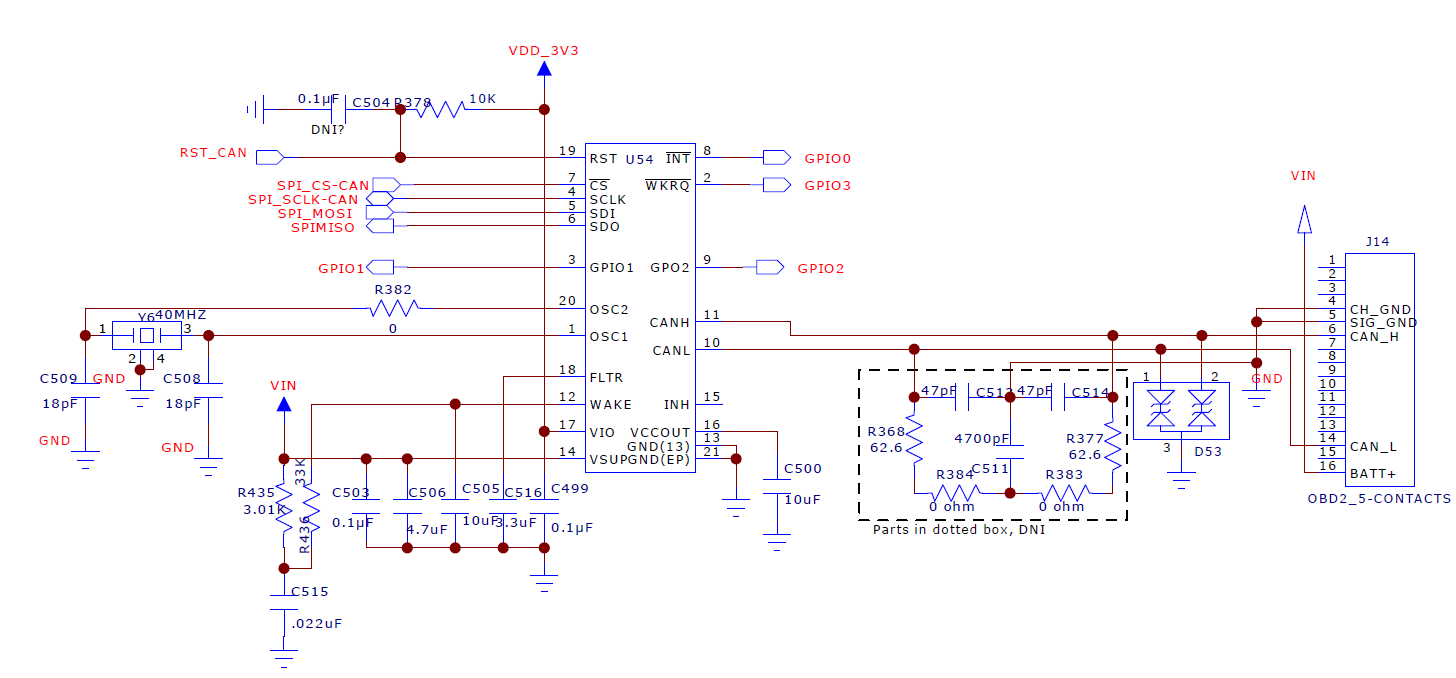
Can you review this schematic and let us know if you recommend any changes?

Thanks,

Brian 

  • Hi Brian,

    I saw a few things that we might want to comment on.

    - The 10k pullup resistor on RST_CAN should be changed to a pull down or be made a DNI. The pin should be low for normal operation and momentarily pulsed high to cause a reset event. As drawn the device will be held in reset unless the other device connected to RST_CAN is constantly sinking current, which is unnecessary. The device already has a weak internal pulldown that should suffice and be easily over driven high by any normal digital IO pin.

    - nINT and GPO2 are open drain architecture and will require a pullup resistor somewhere on the line for a “high.” nWKRQ could be make to be open drain that would require a pullup resistor, otherwise it is ok as drawn if the internal 3.6V reference voltage is acceptable. It's not clear if there will be pullup resistors elsewhere in the schematic, or internal to an MCU, but they should ensure there is a pullup on these lines.

    - The 3.3uF cap on FLTR is larger than the 0.33uF recommended value.

    - It appears that the WAKE pin functionality is not going to be used. If so, the resistor divider is not needed and the WAKE pin can simply be tied high or low since it is a bi-directional input pin. The divider resistor values of 3k and 33k were chosen to limit current when the WAKE pin is used and don't have to be kept if they simply want to tie the pin off. I.e. they could have a single pullup resistor to VSUP and a 22nF cap to GND. The 10uF cap on WAKE is not necessary.

    - I always like to mention that some automotive applications require a certain level of emissions compliance and if so an optional common mode choke could be placed on the CAN pins, or 0-ohm resistors could be installed across the pads of the choke footprint if the choke is not needed. But this is optional depending on the system application requirements.

    -They also don’t have any polarity protection diodes on the VIN line. I’m not sure if there is protection on the other side of the OBD2 contacts that make it unnecessary at this level, but they might want to add a series diode to protect against reversed battery cables. Also, the TCAN4550 has an absolute max input voltage spec of 40V. A clamping diode could be added to prevent any potential damage resulting from a voltage spike on the battery line. These are simply optional recommendations to be considered at the system level.

    Regards,
    Jonathan