This thread has been locked.

If you have a related question, please click the "Ask a related question" button in the top right corner. The newly created question will be automatically linked to this question.

TUSB1064: USB3.0/DP Issue with TPS65987D+TUSB1064 on the sink side

Part Number: TUSB1064
Other Parts Discussed in Thread: TPS65987D, , TPS65987

Dear Sir,

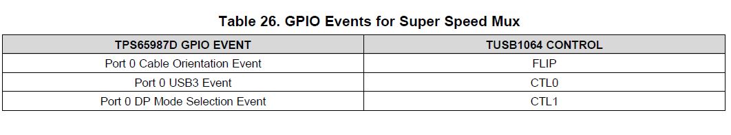
We have a cusomter using TPS65987D +TUSB1046(Source side) and TPS65987D+TUSB1064(Sink side). and currenlty the source side work ok(setting volagte output 5V,12V correct and USB3.0/DP work fine with USB3.0 decve and DP input moniter). And then they connect source and sink side together, we can see the voltage output correct(5V, 12V) and also have USB2.0 singal. However, we can't dedect the USB3.0 and DP singal though TUSB1064. Currenlty , we set the TUSB1064 GPIO(FLIP,CLT0,CLT1) pin as below(according to TPS65987D spec). Could you kinldy adivse us what might cause this issue? we attach the schemaitc and the Sink side TPS65987D configuration file  as your reference

Also, may we have your suggestion about the ADCIN1 setting when it is sink sink side?(support USB3.0 and 2 lanes DP). below is the EVM suggestion schemaitc. When we use 316K, but it seems sink side won't work(only 5V , no 12v votlage dedected) , we change to 20K instead, then the 12V will be detect on the sink side. coudl you kindly suggesiton us the probably resistance on the ADCIN1 pin?thnaks  

Above, please kinldy give us your suggestion and if there is any question, please feel free to contact with me

     TPS65987DDH_new-1108.pjt

Sink_docking board_1009.pdfSource_TI_TypeC_0918.pdf

  • Alec

    Looking at the TUSB1064 schematic.

    TUSB1064 SSTX is input while SSRX is output, so SSTX needs to be connected to SSRX of the connector while SSRX needs to be connected to SSTX of the connector.

    For SSTX, please use 0.33uF instead 0.1uF for ESD purpose. For SSRX, please use 0.22uF.

    For DP, AUXP/N need to be connected straight to the DP source connector since the AC coupling and termination are done inside the monitor. But please check the AUXP/N common mode voltage, AUXP common mode voltage needs to be between 0 and 0.4V and AUXN common mode voltage needs to be between 2.7 and 3.6V.

    Thanks
    David

  • Hi, Daivd

    Thanks for the reply. We do the modification on the SSTX and SSRX.and also remove the o.1uF as your mention. However, ths issue is still not solved. we still didin't get the DP and USB3.0 working(USB2.0 is fine)

    Could you kinldy give me other suggestion which might cause this issue?thanks in advance

    Alec

  • BTW, we also check the AUXP/N common mode voltage. it looks within the spec.
  • Alec

    Let's focus on getting USB3.0 working first.

    It is easier to debug in TUSB1064 I2C mode than in GPIO mode. But if you are using GPIO mode, manually tie CTL0 high, CTL1 low, and FLIP either high or low depends on the cable orientation. You can do the same in I2C mode by writing to register 0x0Ah. This will bypass the PD controller and focus only on TUSB1064.

    You can then probe the output of TUSB1064, are you seeing USB LFPS? If you are seeing LFPS, then at least the USB3.0 handshake is happening, and then we need to focus on the USB3 signal quality. You need to tune the EQ while looking at the TUSB1064 output and make sure you have a USB compliant eye diagram. If you are blue wiring to fix the SSTX/SSRX swap issue, the signal quality could be so bad that USB3.0 may not work.

    Thanks
    David

  • Dear David,

    Sorry to bother you again. we are able to make customer's TPS65987D works with the DP 2 lane +USB3.0 mode. However,when RD is testing DP 4 lanes function,  it seems  the TPS65987D GPIO(control CTL0,CTL1,FLIP pin) wouldn't control TUSB1064 into the 4 lanes DP mode.the connection and configure setting are follow the spec suggestion shown as below. Could you kindly give us some suggestion for this issue?thanks in advance

    BRs

    Alec

  • Alec

    Would you please check to see if multi-function bit in the PD controller is enabled? If multi-function is enabled, then PD controller will configure TUSB1064 as 2 lane DP + USB. Please disable multi-function bit first.

    Thanks
    David
  • HI, David,

    The customer currently is using the GPIO mode. Could you kindly let us know where to set the mutli-function bit that you mention in your previous reply?

    Also, RD currently is testing the TPP65987D power performance . Using their source board(also use TPS65987D) +TPS65987D EVM as sink side, the max load for 5V can reach 5A , However, using the same source board+ their sink board(using the same configuration as TI EVM). the max load only up 3A. could you think of anything might cause this condition? 

    above, hope to hear form your feedback soon

    BRs

    Alec 

  • Alec

    I am referring your question to our PI team since the question is related more to TPS65987 than TUSB1064. The multi-function bit is programmed in the TPS65987.

    Thanks
    David
  • Hi Alec,

    The multi function bit is set in the Display Port configuration register.

    Thank you,
    Eric
  • Hi, Daivd,

    We are able to make the display port work now. We found out the abnormal issue casuse by the AUXp and AUXn. According to the spec as below, AUXp need to be pulled up to DP PWER with 1M resistor and AUXn is pulled up to GND with 1M resistor. But acutally ,it should be the other way around. (the DP funcation works ok after we modfiy it). Now our cusosmer is questioning our spec  and we might nee you hlep to hlep us explain to the customer about this.  please give us some of your advise about this issue.thanks in advance

    Hope you heard form you soon

    BRs

    Alec

  • Alec

    AUXp needs to be pulled up to DP Power with 1M resistor and AUXn needs to be pulled down to GND with 1M resistor. This is part of the DP spec requirement.

    If you look at the entire DP AUX bus implementation per the DP spec, AUXp on the source side needs to be pulled down to GND with 100k resistor while pulled up with 1M on the sink side, this will result ~0.3V voltage on AUXp. AUXn on the source side needs to be pulled up with 100k resistor while pulled down with 1M on the sink side, this will result ~3V voltage on AUXn.

    It looks like the source side does not properly populate the 100k pullup/pulldown resistor, then having 1M pullup on AUXp and 1M pulldown on AUXn would result in 3V on AUXp and 0V on AUXn, which is not correct.

    Thanks
    David
  • Hi,David,

    Thanks for the advise. We will check with the cusotmer with this again.

    Again, thanks for the great hlep

    BRs

    Alec