This thread has been locked.

If you have a related question, please click the "Ask a related question" button in the top right corner. The newly created question will be automatically linked to this question.

SN65HVD72: Inquiry

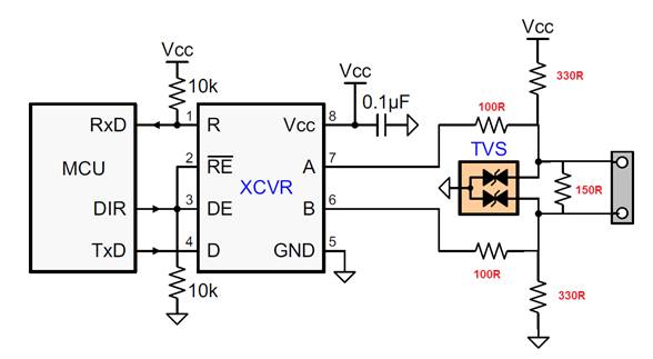
Part Number: SN65HVD72

Hi Team,

I got a question from my customer if it is okay to implement the SN65HVD72 using the below diagram with the additional resistors and Vcc? 

Thanks! 

Best Regards,

Alfred

  • Alfred,

    This may still work, but having 100-Ohm series resistances in conjunction with 150-Ohm termination will attenuate the RS-485 signaling significantly (by more than 70%, assuming dual termination is used). This would limit the cable lengths that could be supported, since there is no budget for additional loss through the cable. Generally it would be better to keep the series resistances less than 10-20 Ohms for a terminated bus.

    What are you trying to accomplish with this resistor network?

    Regards,
    Max
  • Hi Max,

    Thanks for the feedback! This is the feedback I got from customer:

    The series resistor is for surge/lightning protection. The rest of the network resistor is end customer implementation, not sure why it’s done that way.


    So if we change the series resistor to 10R, you don’t see any potential problem anymore?

    Thanks! 

    Best Regards, 
    Alfred


  • Hi Alfred,

    Sorry for the delay, last week was a holiday in the US.

    It's true that a series resistance can be effective in improving the surge/lighting immunity of a system by limiting the current that could flow into the transceiver when an over-voltage condition exists. Reducing the series resistance to 10 Ohms would mean reduced immunity, although it may still meet the overall application requirements. What surge specification is targeted for this design?

    If reducing the series resistance results in inadequate surge immunity, then there are a few different options that could be evaluated. One would be to keep the circuit as-is with the higher resistance values and evaluate the signal integrity to make sure it is sufficient even for worst-case cables. Another would be to remove the termination resistances or increase their value so that there is less attenuation across the series resistances. A third strategy would be to implement a more complex transient protection scheme (e.g., transient voltage suppression diode, metal oxide varistor, gas discharge tube, etc.). A fourth would be to use a transceiver with higher transient immunity.

    Best regards,
    Max
  • Hi Max,

    Thanks for the feedback! Really appreciate it! Customer said they will implement 10R series resistor and qualify actual unit, they will adjust value on need basis depending on test result.


    Regarding pull up and pull down, I assume there is no concern even though not included in IC application note.

    Can you help confirm that this assumption is correct?

    Thanks! 

    Best Regards,

    Alfred

  • Alfred,

    Yes, the pull-up and pull-down resistances are OK to include and are useful for establishing a valid differential "high" level when all of the drivers on the bus are disabled. This technique is often referred to as failsafe biasing, and if you are interested you can read more about it here:

    e2e.ti.com/.../rs-485-basics-two-ways-to-fail-safe-bias-your-network

    www.ti.com/.../slyt324.pdf

    Best regards,
    Max
  • Hi Max,

    Thanks for the support! I am closing this thread. 

    Best Regards, 

    Alfred

  • Hi Max,

    I received an additional inquiry about this, can you share more details about the internal biasing for open fail-safe protection.

    Our customer wants to dig in on this. The specs shows little information regarding internal bias on the pin A and B.

    Thanks! 

    Best Regards, 

    Alfred Logico

  • Hi Alfred,

    Sure. Rather than biasing the A/B pin voltages, this device implements a small offset voltage in the receiver's comparator circuit (i.e., what is used to determine whether the input differential voltage should be considered high or low). This has the effect of shifting the effective switching threshold voltage. This can be seen in the VIT+ (positive-going receiver threshold) and VIT- (negative-going receiver threshold) specifications. That than being centered around 0 V (no offset), both thresholds are defined to be negative. This means that if there is a condition like an open bus that results in a differential input voltage of 0 V, this input level will be considered a "high" rather than an indeterminate state.

    I hope this helps - let me know if it is unclear.

    Best regards,
    Max
  • Hi Max,

    This is great! I will let you know if customer has additional questions.

    Thanks! 

    Best Regards, 

    Alfred

  • Hi Max,

    Here is the feedback of customer:

    This was mentioned in your specs as well as on the app notes. On the other hand, can you show thru block diagram how the internal biasing was implemented. Is it thru pull up/down resistor or level shifter.

    Thanks!

    Best Regards,
    Alfred
  • Alfred,

    The biasing is not implemented via pull-up/pull-down resistors (as it might be implemented externally). The receiver input acts as a comparator (in order to convert the differential signal at the input into a logic high or low level), and the first stage of this circuit is basically a high-gain differential amplifier. A small offset bias current is introduced on one side of this amplifier in order to effectively produce an input offset voltage. Since this implementation is within the comparator itself, an offset voltage may not be visible externally. This means that the internal failsafe biasing applies only to this transceiver and would not be carried over to all other nodes on a network (like it would if pull-up/pull-down resistors were used).

    Hope this makes sense - I can't go into much more detail due to confidentiality concerns. Let me know if you have any further questions, though.

    Max