This thread has been locked.

If you have a related question, please click the "Ask a related question" button in the top right corner. The newly created question will be automatically linked to this question.

TINA/Spice/DS90UB934-Q1: IBIS model showing ROUT lines response showing greater than 50% duty cycle when provided input duty cycle is 50%?

Part Number: DS90UB934-Q1
Other Parts Discussed in Thread: TINA-TI

Tool/software: TINA-TI or Spice Models

Hi Team,

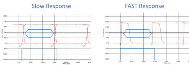
My customer is seeing the following when using the x934 de-serializer IBIS model.

Issue observed:

Deserializer ROUT lines response during Fast corner and Typical corner are having an issue of having duty cycle more than 50%, whereas the provided input duty cycle is 50%.


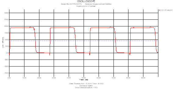
FYR, Fast Response with Stimulus provided:  Oscillator of 37.125MHz

  • Hello,

    The distortion of the Deserializer output, is strongly affected by the board trace, capacitance, and load resistance.

    I have attached a ADS IBIS simulation of the R0 output with a 2K load resistance, and 20pf capacitance.   The datasheet

    indicates the output drive is specified at 4ma (see datasheet).

    I have included the ADS schematic, the ADS plot, changing the output trace, resistance and capacitance (and trace features) will change the output.

    I think the waveform growing 5-10% in dutycycle is not as important, the Output clock and Data traces being matched length, or lengthening the output clock

    to meet more setup time at the receiver should be reviewed.

    ADS schematic

     ADS plot

    Regards,

    Joe Quintal

  • Hi Joe,

    Thanks for the detailed response. From your comments, the duty cycle change should not be an issue in the simulation but when i look at the provided waveform the fast response is overlapping reducing the eye of this high speed signal.

    Also, Can you explain on your comment regarding giving more setup time on the receiver? Not sure what this is referring to.
  • Hello
    The outputs of the 934 are digital logic, and a separate clock (PClk), the eye diagram is not normally used for a parallel set of LVCMOS signals.
    The R11-R0, HSYNC, VSYNC are registered with PClk in the customer device. The customer device Tsu and Thi, around the PClk transition,
    including jitter are evaluated to register the data. In the 26ns period range. where the half period clock transition is used at the receiver. The data with all of the Signal Integrity settles to the new value in about 5ns. If the receiver device has a Tsu and Thi of 2-3ns. This leaves a 5ns margin. If you made the PCLK 1ns longer than the data traces, you would have more setup time. It is not needed in this example.

    The layout should have a matched length of data R11.R0, HSYNC, VSYNC, and PClk to with ~1ns. Since this is LVCMOS 3.3v, trace width of each bus signal is based on receiver characteristic impedance, there should be a spacing from each output signal and clock to other signals. Ideally routed as striplines over a GND or Power (uncut) plane. This would provide timing margin of ~4ns for layout, and could be measured to compare with IBIS simulation on the customer board.

    Regards,
    Joe Quintal
  • Hi Joe,

    Thanks for the detailed response, its clear to me now. I did want to add that an increase in duty cycle in the IBIS model is only observed in fast mode. Also effects of the PCB were not considered, only 1Mohm termination and input capacitance of the load IC as termination.