Part Number: SN65DSI85
Hi,
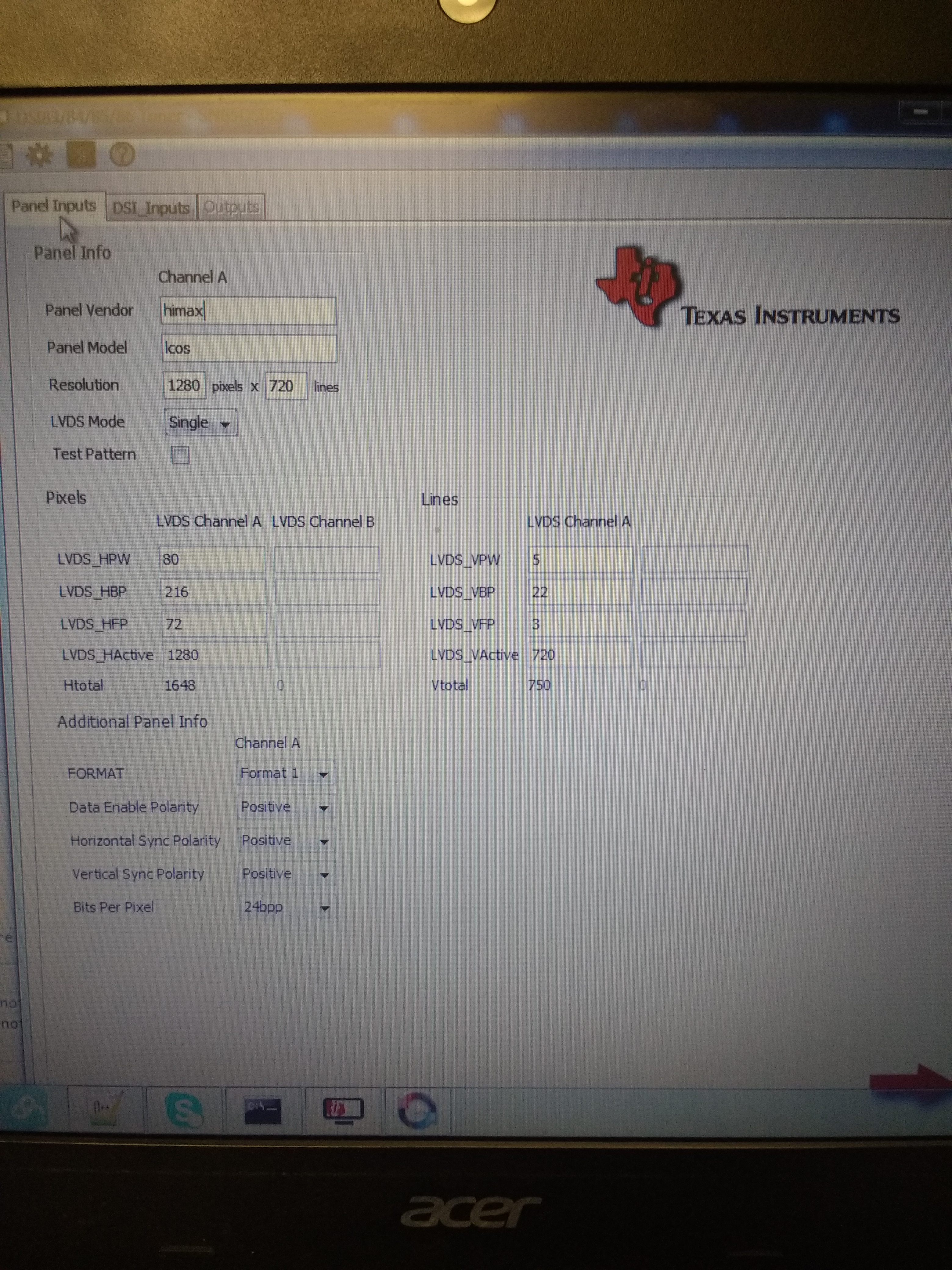
We are using SN65DSI85 for single DSI to single LVDS, i.e. we are using Channel A to Channel
The panel resolution info is as below:
HTotoal = 1648 = [1280(Active) + 80(HPW) + 216(HBP) + 72(HFP)]
VTotoal = 750 = [720(Active) + 5(VPW) + 22(VBP) + 3(VFP)]
Frame rate = 60Hz
We are using ref clock as 74.25. *** DSI CLK is not used for generating LVDS clock******
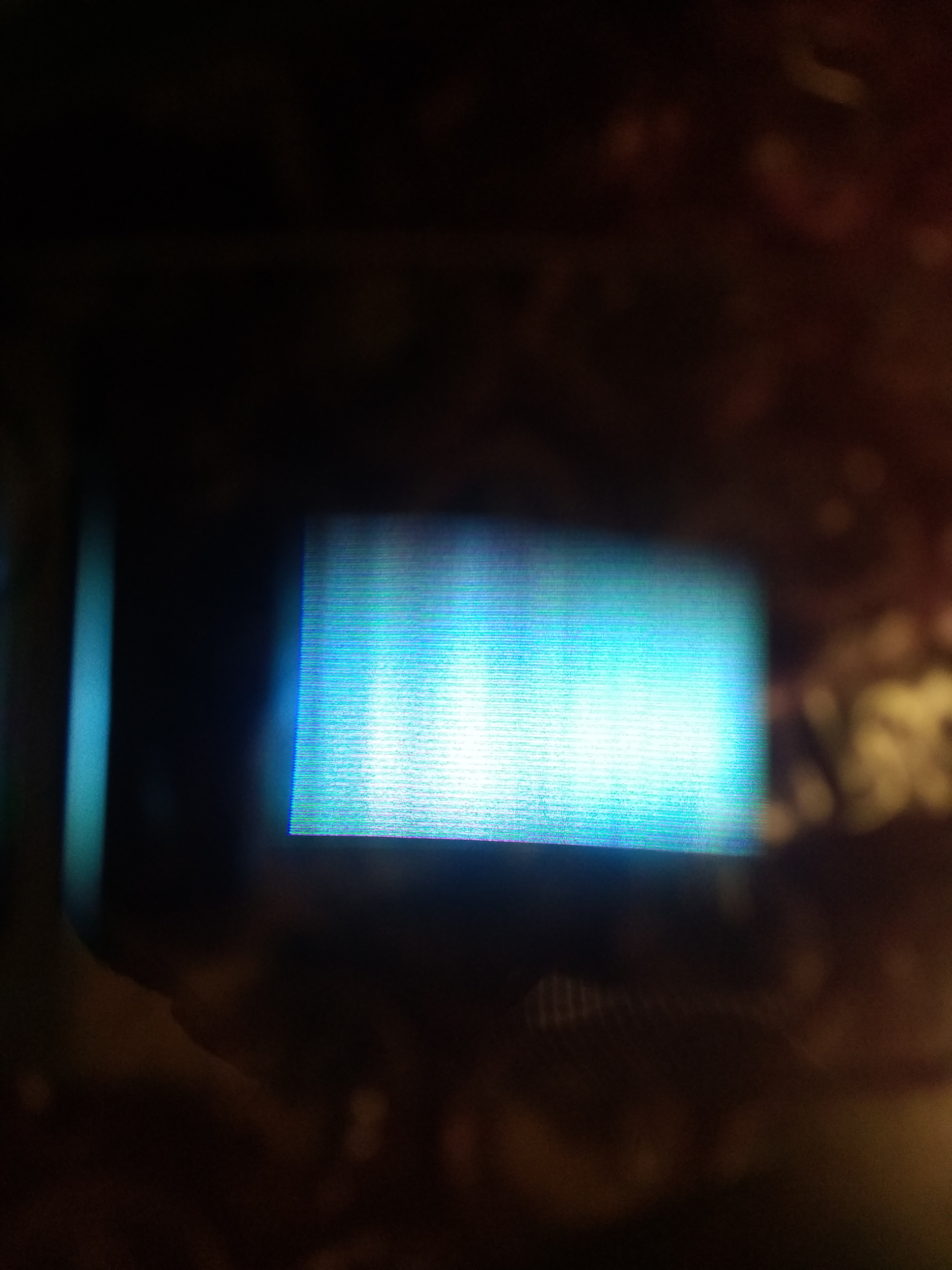
We see the test pattern being displayed on the panel correctly. However garbage is being displayed when we drive data from DSI. Attached is the snapshot of what it looks like.
Also attached is the register dump. Can you please let us know if we are doing something wrong!!
[0x9] -> [0x0]
[0xa] -> [0x84]
[0xb] -> [0x0]
[0xd] -> [0x1]
[0x10] -> [0x20]
[0x11] -> [0x0]
[0x12] -> [0x2c]
[0x13] -> [0x0]
[0x18] -> [0x1a]
[0x19] -> [0x0]
[0x1a] -> [0x3]
[0x1b] -> [0x0]
[0x20] -> [0x0]
[0x21] -> [0x5]
[0x22] -> [0x0]
[0x23] -> [0x0]
[0x24] -> [0xd0]
[0x25] -> [0x2]
[0x26] -> [0x0]
[0x27] -> [0x0]
[0x28] -> [0x20]
[0x29] -> [0x0]
[0x2a] -> [0x0]
[0x2b] -> [0x0]
[0x2c] -> [0x50]
[0x2d] -> [0x0]
[0x2e] -> [0x0]
[0x2f] -> [0x0]
[0x30] -> [0x5]
[0x31] -> [0x0]
[0x32] -> [0x0]
[0x33] -> [0x0]
[0x34] -> [0xd8]
[0x35] -> [0x0]
[0x36] -> [0x16]
[0x37] -> [0x0]
[0x38] -> [0x48]
[0x39] -> [0x0]
[0x3a] -> [0x3]
[0x3b] -> [0x0]
[0x3c] -> [0x0]
[0x3d] -> [0x0]
[0x3e] -> [0x0]
[0xe0] -> [0x0]
[0xe1] -> [0x0]
[0xe2] -> [0x0]
[0xe5] -> [0x1]
[0xe6] -> [0x0]
Regards,
Vijay