This thread has been locked.

If you have a related question, please click the "Ask a related question" button in the top right corner. The newly created question will be automatically linked to this question.

SN65HVD1781: Attached circuit for the switching between two interface. Suggest

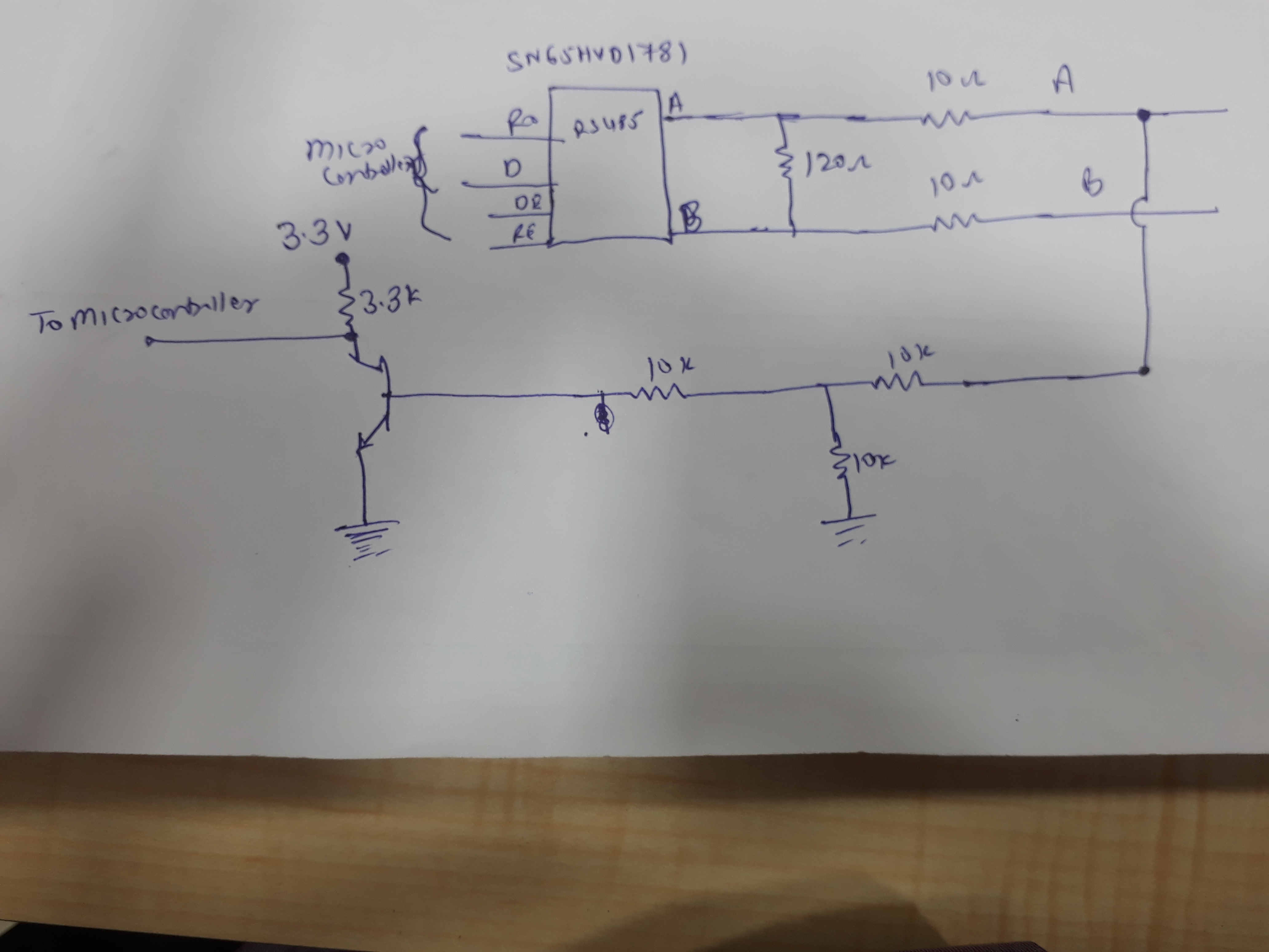
Part Number: SN65HVD1781

Hi,

Attached is the image of circuit in which I am using RS485 Transceiver "SN65HVD1781". Please note that necessary protection for ESD/EFT are not shown in image.

In my requirement there is another optional signal on line "A" of maximum amplitude of 24V (in that case there is no RS485 communication and also no other RS485 device) .

If there is RS485 communication then other signal devices are not there.

Through Channel "A" I have made separate line for the resistor divider and applied this signal to micro through transistor as shown in figure for detecting 24v signal.

Let me know what would be the impact On RS 485 signal due to added separate path when RS485 signal is present and no other signal. 

Thanks

  • Hi,

    If you're concerned the symmetry of the bus line, you could add another path with the same resistors on B pin. Please make the both paths short therefore the 'stub' is not long enough to generate some reflection. BTW, with the resistor divider, the gate of the BJT would see 12V with 24V showing on A. Please make sure it's within the BJT's work range.

    Please let me know if you have more questions. Regards,

    Hao

  • Hi,
    My concern is on following things.
    1. As same channel is used for RS485 and if mode is RS485, then does there any effect of voltage divider and other circuitry on channel A.
    I can not mount same divider circuitry on channel B as when there is no RS485 then channel B worked as GND as a reference for 24V digital input.

    Intention is to used same A and B line as either for RS485 or 24V digital Input based on some software configuration.
  • Hi,

    The resistors (voltage divider) can be considered a 20kOhm pull down to ground. RS-485 communication should still work provided that there are not many nodes in your application. The same analysis applies to B side as well. Please let me know if you have more questions.

    Regards,

    Hao  

  • One minor point - the weak pull-down on the A line should result in a slightly lower voltage on "A" compared to "B" if no transmitters are active on the bus. This could be interpreted by a receiver as a logic "low" level on the RS-485 bus. If that is problematic for the communication protocol used, then you could either place the full-down on the "B" line instead or introduce other pull-up/pull-down resistances on the A/B lines in order to provide a small positive differential bias when the bus is idle.

    Regards,
    Max
  • Hi,

    As I told earlier When RS 485 is not used it will be disabled through RE and DE. During this time Channel "B" there will be GND and on channel "A" there will be 24V from outside as a digital input.

    So for digital input configuration RS485 will be in disable state. So same channel "A" has another stub going to micro-controller through multiplexer and transistor (24V is divided to 12V before fed to multiplexer due to max voltage limit of MUX) and then through transistor to microcontroller as a digital input.

    I just wanted to sure that the scheme defined by me will work for RS485 (RS485 is enabled. And Digital input mode is disabled through MUX).

    Thanks

  • Hi,

    Your scheme should work for RS-485 communication, provided the stub on channel "A" is not too long. The rule of thumb is "The electrical length of a stub (in foot) should be shorter than 1/10 of the driver’s output rise time (in ns)" (section 6 in this application note). I don't see any issue in DC level other than the minor point Max mentioned. Please let us know if you have more questions.

    Regards,

    Hao