This thread has been locked.

If you have a related question, please click the "Ask a related question" button in the top right corner. The newly created question will be automatically linked to this question.

TLK10232: TLK10232: Clock output is not coming from TLK10232CTR bad signal

Part Number: TLK10232

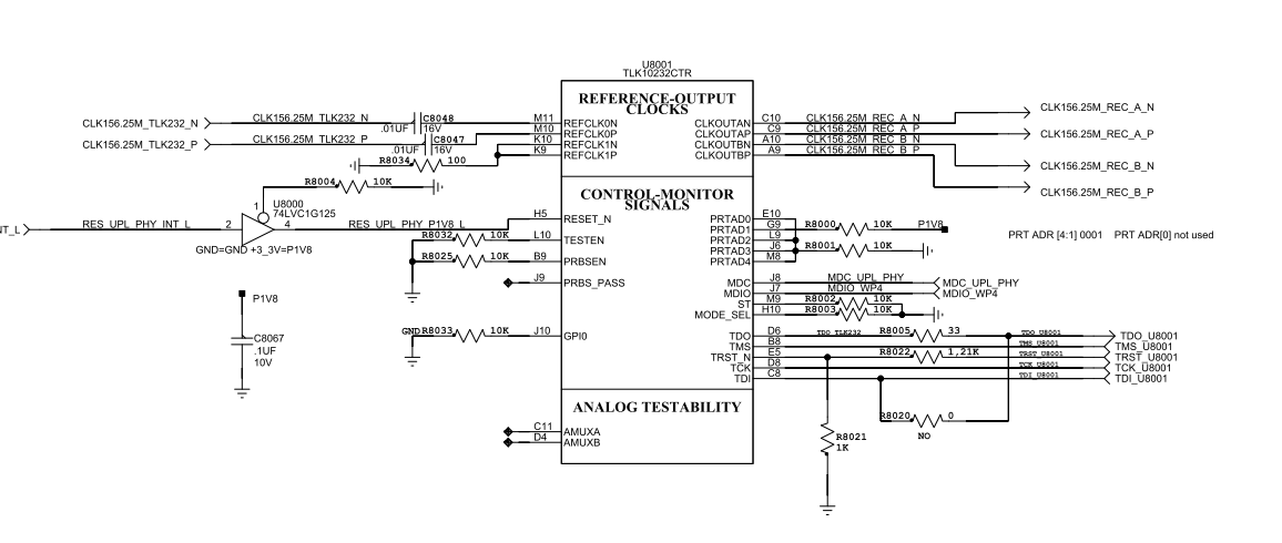
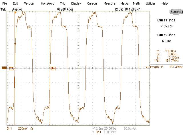
Update for https://e2e.ti.com/support/interface/f/138/t/744224

We measured frequency from TLK10232 ,  it's not correspond to our expectation ( 161.3  != 156.25 MHz)

Please tell a solution to receive the expected 156.25 MHz.

  • Taras,

    Could you again provide the reference clock input to TLK10232 and the register settings for CLK_CONTROL?
  • Ok, please look

    dev 0x1e reg 0x1d  value  0x0
    REFCLK_FREQ_SEL_1    = 0
    REFCLK_FREQ_SEL_0   = 0

    dev  0x1e reg 0xd  value 0x2f80
    CLKOUT_SEL       00x0 = Selects Ch A HS recovered byte clock as output clock

    CLKOUT_DIV       1000 = Divide by 4 (Default 4'b1000)

    CLKOUT_ EN        = 1      Allows CLKOUTx_P/N output to toggle normally

                        CLKOUT_POWERDOWN  0 = Normal operation (Default 1’b0)

    dev 0x1e reg 0x2 value 0x831b
    HS_ENPLL = 1 Enables PLL in HS serdes (Default 1’b1)

     dev 0x1e reg 0x6 value 0xf114

    LS_ENPLL 1 = Enables PLL in LS serdes (Default 1’b1)

    LS_MPY = 0100     8x

     dev 0x1e reg 0xf value 0x1403

    HS_PLL_LOCK = 1

    LS_PLL_LOCK= 1

     dev 0x1e reg 0x7 value 0x0

    LS_RX_RATE =0      00 = Full rate (Default 2’b00)

    Malik Barton57
    Also when testing are you providing input data to the device?

    Yes we send 100 packets  after that we get

              HS_PLL_LOCK = 1

    LS_PLL_LOCK= 1

  • Taras,

    When testing are you sending valid data to TLK10232 as that a byte clock can be recovered?
  • Hi,

    What do you mean "valid" ?

    packets has valid source and destination  , crc ,  but custom type.

    packets are sending throw an eth-switch.

    Could be a problem with rate setup in register 0x1e 0x07 ?

  • Hi,

    I thinks that your problem is :
    CLKOUT_SEL 00x0 = Selects Ch A HS recovered byte clock as output clock

    In my case, i don't know why parameter CLKOUT_SEL = 00x0 and CLKOUT_SEL = 10x0 don't works.

    I see that your clock input = 156.25MHz
    If it's 156.25MHz and you want 156.25MHz for CLKOUT P/N so you can use these parameters (works for me) :
    CLKOUT_SEL = 1111 (or eventually 0111)
    CLKOUT_DIV[3:0] = 0100 (divide by 2).
  • Hi,

    so you suggestion is to take signal from LS side ?

    I considered, in this case, you use the same internal oscillator for all parts of your board, isn't it ?

  • Hi Taras Shevchenko,

    Sorry but I'm not understant your question.

    In my case 156.25MHz is connected to Refclk0P/N like your schematic.

    In REFCLK1 P/N i have a second 156.25MHz clock but i don't use it (REGISTER 0x1E.0x0001 bit (1) REFCLK_SW_SEL = 0).

    With parameters that i gave you, CLKOUT(A) and CLKOUT(B) = 156.25MHz.

    My LS side is connected to a FPGA. So In my fpga i use CLKOUT(A/B) as clock input.

    Clkout (A) is an input clock for channel A LS side & CLKOUT(B) is an input clock for channel B LS side.

    And FPGA use CLKOUT(A/B) to generate 3.125Gbp/s data in the LS SIDE (in my case i use it in a 10GB-KR application). 

    About HS side clock, it's just necessary to configure pll multiplier of  HS_SERDES_CONTROL_1 register.

    in my case HS_PLL_MULT[3:0] = 1100 (PLL Multiplier factor = 16.5).

  • Sorry, it is possible that I miss some details
    As I understood , main task is to be synchronous with upper device. So we should take signal from uplinks to synchronize our device.
    You take signal from LS side connected to FPGA and send it back to FPGA as clock input ? It looks like a loop.
  • I don't know how is your configuration.

    I only see that you have a problem with the value of your CLKOUT (A) pin.

    In the past, i had problem me too with the value of my clkout frequency. So i advice you to check the CLKOUT_SEL value. CLKOUT_SEL was my problem.

    Can you please send a schematic like the picture in attachment because i have difficulty to understand your question. Why do you speak about loop.

    Here schematic of my system.

    1/ At startup, FPGA configure all register of TLK10232 by MDC / MDIO bus.

    2/ When configuration is finish, CLKOUT(A/B) = 156.25MHz. TLK10232 use REFCLK0 (not connected to FPGA) to generate clock at FPGA.

    The combination of 156.25MHz TLK10232 input (refclk0)  and register configuration give a 156.25MHz at CLKOUT(A/B) pin.

    3/ FPGA clock input is 156.25MHz and use this frequency to generate 3.125Gbps data on the LS side. HS side run @10 gbps due to TLK10232

    If i correctly understand your configuration. 

    1/ TLK10232 is 156.25MHz

    2/ You want CLKOUT(A/B) = 156.25MHz but channel clkouta= 161.3MHz

    3/ So try to configure :

    CLKOUT_SEL = 1111 (or eventually 0111)
    CLKOUT_DIV[3:0] = 0100 (divide by 2).

    And check the frequency of your clock CLKOUTA.

    For me the configuration CLKOUT_SEL = 00x0  or 10x0 (i don't know why). So try others value for clkout_sel in the goal to know if it's your problem.

    i recommend you the same value that me because it works for me.

    CLKOUT_SEL = 1111 (or eventually 0111)
    CLKOUT_DIV[3:0] = 0100 (divide by 2).

    You can use others value for CLKOUT_SEL (ecxept for 00x0 and 10x0) but you need to correctly configure CLKOUT_DIV.

    Can you only try to modify this value 

    CLKOUT_SEL = 1111 (or eventually 0111)
    CLKOUT_DIV[3:0] = 0100 (divide by 2).

    and check your CLKOUTA frequency. If you always have 161.3MHz, so you have a problem different that me.

  • Hi,

    Could you add some details to your schematic ?

    Source for refClk0 ?

    What source FPGA used until TLK10232 configuration ?

  • Hi,

    Source for refclko = Silicon Labs SI510 CRYSTAL OSCILLATOR.

    FPGA use an others oscillator (25MHz) for only MDIO communication. This clock is always active after power is on.

  • In my case :
    internal OSC -> si5345->refclk0 and clckout from TLK10232 -> si5345 . on si5345 I can select clock source
  • Hi,
    1/ You configure your SI5345 in the goal to obtain 156.25MHz for refclk0
    2/ You check that your refclk0 frequency is correctly set at 156.25Mhz (with an oscilloscope).
    3/ You configure your TLK10232 and for the 2 registers below you use these value :
    CLKOUT_SEL = 1111 (or eventually 0111)
    CLKOUT_DIV[3:0] = 0100 (divide by 2).
    4/ You check that clkout from TLK10232 is correctly set at 156.25MHz or not (with an oscilloscope).

    So after step 4 :
    -- if clkout = 156.25Mhz, your problem was CLKOUT_SEL and CLKOUT_DIV values.
    -- if Clkout = 161.3MHz, CLKOUT_SEL and CLKOUT_DIV registers was not your problem.
    You have an other problem that you need to find.
  • Taras,

    Does the previous post help your issue? What do you see after step 4?
  • Need more time to check

    answer asap

  • Taras,

    I will be waiting on your reply.
  • Taras,

    Is there any more support needed for this issue? If so please reply with any relevant details so that I can further assist you. For now I will be marking this thread as "TI Thinks Resolved". If you have resolved your issue, please post the solution to the original problem/post for others with similar issues.
  • Thank you, for supporting

    We decided to  increase thresholds on Si5345 and now try to do some other manipulation with it.

  • Taras,

    Please let me know if more support is needed.