A related question is a question created from another question. When the related question is created, it will be automatically linked to the original question.
If you have a related question, please click the "Ask a related question" button in the top right corner. The newly created question will be automatically linked to this question.
The datasheet shows that the BYP needs to connect a 0.2uF to increases the ESD. When we add the large Cap at BYP, seems the BYP will be damage by ESD. Can you guide me it? Thanks!
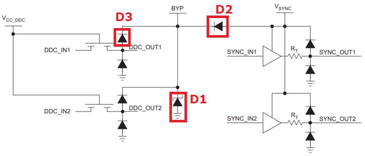
There is a high speed shotkey diode shown in the datasheet that is there to protect the BYP pin and provide additional support to all of the other ESD structures.
The BYP cap should be rated to at least 50V to give headroom for the diode protection scheme and to provide the best derate value.
If this fully answers your question, I would appreciate you clickin the customer thinks resolved button or ask any further questions you might have.
Hi Chuck,
You pointed out the key point, the fail device is installed the 22uF/6.3V Cap at BYP, but in the TPD7S019 is only 5V, why TPD7S019 will be damage, but not Cap.
The BYP pin will absorb charge from all of the other pins and during the ESD event may exceed 5V for a short period of time. I prefer to use a higher voltage rated cap for this reason. The only reason that I know of that the cap could cause the device to fail is if there is too high of an impedance between the pin and the capacitor.
Are you able to send me the layout of the PCB as a private message so I can take a look at it?
It would also be helpful for me to see your ESD test procedure as well.
I would like to help with your debug as much as possible.
I am attempting to get you answers on these questions. The data is not part of the datasheet so if I am able to get access to it, it will take a few days to obtain.
I have finally located a contact on this part and I am reaching out today to get these questions answered. I should have information for you by Thursday at the latest.
Here is the guidance we can provide. Note that TI cannot recommend any condition beyond the abs max in the datasheet.
• The reverse breakdown of these diodes is on the order of:
o D2, D3 VRB=~12V-14V
o D1 VRB=~7V-8V, has some snap-back as depicted in Figure 1 of the datasheet.
• D3 is designed to handle 8kV IEC pulses (~16A at ~30nS pulse) in the forward direction. Longer pulse data is not available for this device, but similar devices have been tested to withstand ~4A at 20us pulse length. This diode is not designed for DC forward current. This diode is not designed to handle any significant current in the reverse direction.
• D1 is designed to handle 8kV IEC pulses (~16A at ~30nS pulse) in both the forward and reverse direction. Longer pulse data is not available for this device, but similar devices have been tested to withstand ~4A at 20us pulse length. This diode is not designed for DC forward current.
• D2 is designed to handle 8kV IEC pulses (~16A at ~30nS pulse) in the forward direction. Longer pulse data is not available for this device, but similar devices have been tested to withstand ~4A at 20us pulse length. This diode is not designed for DC forward current. This diode is not designed to handle any significant current in the reverse direction.
If this fully answers your questions, then please click the customer thinks resolved button.