This thread has been locked.

If you have a related question, please click the "Ask a related question" button in the top right corner. The newly created question will be automatically linked to this question.

TCA9517: ACK transmit issue of TCA9517

Part Number: TCA9517

Hi team,

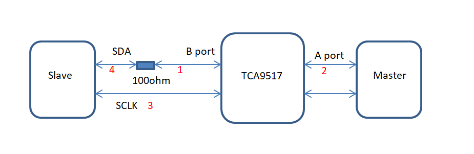
My customer use the TCA9517 as below:

But the TCA9517 can't pass the low voltage from B port to A port that causing the communication failure between the Slave and Master.

Below are the waveform captured by customer:

The Channel 4 is the wave of the slave and Channel 1 is the wave of B port. There is a 100 ohm resister between the slave and TCA9517 causing the voltage of B port is a little higher than the Slave output voltage.

The voltage of the ACK low voltage in B port is about 383 mV.

According to the specs in the datasheet, the 383mV should be recognized as the low logic, but the test result is opposite.

Can you help to provide your comments about this?

Lacey

Thanks a lot!

  • Hey Lacey,

    VoL-ViLc of TCA9517 is a typical 70mV. VoL min is 450mV so if the hysteresis value is 70mV and VoL minimum is 450mV then the ViLc minimum value is about 380mV (450mV-70mV) by assuming a VoL minimum of 450mV.

    Typically we recommend customers not use series resistors on B side due to the offset it generates (like in your condition) and affects the voltage our TCA9517 sees. Just to confirm, does removing and shorting the 100 ohm resistor resolve the issue?

    Thanks,
    -Bobby
  • Hi Bobby,
    Thanks so much for your reply!
    1. According to the calculation you mentioned, why is the typical VILC 400mV as the typical Vol is 520mV, and the typical hysteresis is 70mV.
    (520-70=470mV)
    I just assume customer will ask this question, does the 400mV VILC is the data collected in the production test?
    2. Customer said if reduce the value of the resistor, the issue can be fixed. So can you help to double check the minimum VILC, I may need to ask customer to change a resistor value which can make sure the voltage is lower than the minimum VILC.
    3. So does the circuit in B port is used to eliminate the interruption of some noise? I just curious about why do we just integrate the circuit in the B port?

    Lacey
    Thanks so much!
  • Hey Lacey,

    "1. According to the calculation you mentioned, why is the typical VILC 400mV as the typical Vol is 520mV, and the typical hysteresis is 70mV.
    (520-70=470mV)"
    I understand your concern here, to be honest the math does not make sense to be in terms of the typical values. To me the typical value for VoLB-ViLc should actually be 120mV.... I'm going to have to discuss/work with our design team to see if I can get a better understanding as to why 70mV was used and not 120mV.

    "2. Customer said if reduce the value of the resistor, the issue can be fixed. So can you help to double check the minimum VILC, I may need to ask customer to change a resistor value which can make sure the voltage is lower than the minimum VILC."
    Is Vcc 3.3V on both sides? This likely will influence ViLc to some extent so I need to know Vcc values on both sides.

    "3. So does the circuit in B port is used to eliminate the interruption of some noise? I just curious about why do we just integrate the circuit in the B port?"
    You're asking about why we require a ViLc and why we don't use ViL like on A side correct? The short answer is because we need to make sure the VoL on B side does not redrive the input to drive A side low and latch the bus. So if A side drives B side low, VoLB>ViLc so the device does not redrive itself low and latch up. If VoLB < ViLc then the device would be stuck low forever.

    Thanks,
    -Bobby
  • Hi Bobby,
    Can you help to check the question 1 and question 2 as soon as quickly? It affect the production of my customer.
    For the A port and B port voltage, they are all 3.3V.
    Lacey
    Thanks a lot!
  • Hey Lacey,

    For Point 1:

    I just got the sim data back. The device was designed with a hysteresis value of 70mV so this is why the typical numbers do not add up. VoL-ViLc in the datasheet is not VoLB but rather VoL required on the input to release the device from B side driving low during contention. So 0.4V+.07V is VoL where the contention state is released.

    For point 2:

    From the data I looked at, ViLc stays at a steady 0.4V for almost all cases, I saw some variance at plus and minus 100mV across some weak and strong models. Real silicon will likely have a little more variance so seeing a variance of 200mV (0.38V) could be possible on the outlier cases.

    Also as an alternative, you can also have the customer use TCA9517A as the ViLc of the A revision was designed for 0.45V instead.

    Thanks,

    -Bobby

  • Hi Bobby,
    For the Vol and Vilc, I also can't understand properly.
    For example, the Vol in B port is 520mV. Now the I2C signal transmit from A port to B port, and then the B port is in low state.
    So the voltage of B port is 520mV now.
    The ACK signal is the low voltage from the B port to A port. So if we want the B port to identify the low voltage, because the design hysteresis value is 70mV, and then we need make sure the B port input low voltage should be lower than 520mV-70mV=470mV.
    1. So my concern is that why the typical Vilc of B port is not 470mV but 400mV?
    2. According to calculation, because the range of Vol is from 0.45 to 0.6, can we say the range of Vilc is from 0.38mV to 0.53mV?
    3. In addition, if customer need us to modify the datasheet to indicate the range of Vilc, can we do that?

    Lacey
    Thanks a lot!
  • Hey Lacey,

    I understand this is a bit confusing and the datasheet does not seem to make things clear.

    So VoLB is the low voltage when A side drives B side low. You basically will see a static voltage offset of about 0.52V (more if you have a stronger pull up resistor).

    ViLc is the voltage you need to pull below to make B side drive A side low when A side is in the middle of driving A side low and has yet to release or is in the middle of releasing. (The device has some prop delays so pulling below ViLc is the best way to ensure A side goes low in time). This value is 0.4V (test values suggest the variance can result in a low of about 0.390V in simulation across weak, nominal, and strong models and temperature sweeps).

    Now VoL-ViLc in the datasheet is the hysteresis value and the BASE value for this is ViLc specified in the datasheet. VoL in the case is not VoLB like we discussed earlier. It is the voltage on SDAB/SCLB. Thing of it as the master or slave's low voltage.

    So the device releases when B side goes above ViLc+(VoL-ViLc<--think of this bubble as a constant value designed into the device) or 0.4V+70mV.

    "2. According to calculation, because the range of Vol is from 0.45 to 0.6, can we say the range of Vilc is from 0.38mV to 0.53mV?"
    Let's go off of reported data across many samples as this will be more reliable:

    After looking at data, I've found that ViLC does not exceed 0.42V in simulation and for the minimum value I saw around 0.39V. Real silicon may have further variance though I found char data which shows around .39V and .41V for the variance but I found these values to be rounded. The actual sigma value was around 5mV with a 3 sigma down and the average ranged between .395V and 0.4V (moves with different Vccs) so with this we could actually find a ViLc as low as 0.38V. (I assumed a Gaussian distribution)

    "3. In addition, if customer need us to modify the datasheet to indicate the range of Vilc, can we do that?"
    It would require us to add additional tests to be done for each fabricated device which would drive up cost. Any values which are specified by a minimum and maximum in a datasheet are required to be tested before sale. On our side, we would not want to do this if we don't have to.

    If this device is not suitable because they require a higher ViLc due to the series resistor then we should try to move the customer to TCA9517A as the ViLc is shifted up to 0.45V. <-- Assume the same Gaussian Distribution and a sigma value of 10mV (I basically doubled it which is huge and unlikely but gives worst case) then even at a -3 sigma value, we find the minimum to be 0.42V.

    Thanks,
    -Bobby