This thread has been locked.

If you have a related question, please click the "Ask a related question" button in the top right corner. The newly created question will be automatically linked to this question.

PCF8574: Several questions

Part Number: PCF8574

Hi all

Would you mind if we ask PCF8574?
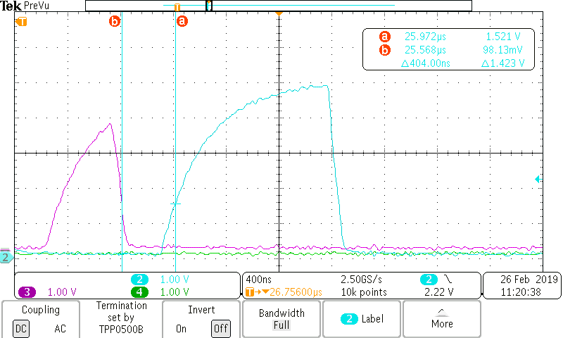
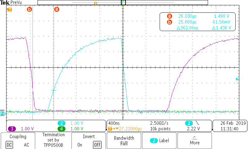
<Question1>
Which of rising edge and falling edge does the device latch their data(input or output)?
We assume that it latches at rising edge.

<Question2>
In relation to follows forum, if I2C frequency is 250kHz, what kind of the problem might it occur?
e2e.ti.com/.../2861237
If you have some advice, could you let us know?
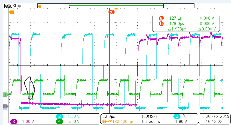
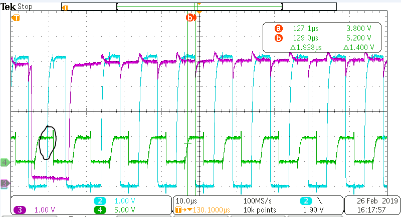
<Question3>
Will IO expanders reflect their values at an ACK condition?

Kind regards,

Hirotaka Matsumoto

  • Hey Hirotaka-san,

    "Which of rising edge and falling edge does the device latch their data(input or output)?"
    Are you asking in terms of when you perform a write when does the output become high or low?

    Or are you asking during a read operation of the input?

    "In relation to follows forum, if I2C frequency is 250kHz, what kind of the problem might it occur?"
    My guess is the device may not ACK because the state machine did not properly receive the signal (SDA/SCL). I would need to do testing on this to confirm though.

    "Will IO expanders reflect their values at an ACK condition?"
    Which values are you referring to? Setting the device as an output high/low?

    May I ask the careabouts of the device is? I am wondering if you need to use PCF8574 or if we can find another IO expander which may fit the application better.

    Thanks,
    -Bobby
  • TRX san

    Thank you so much for your reply!

    Are you asking in terms of when you perform a write when does the output become high or low?
    Or are you asking during a read operation of the input?
    ->We would like to confirm both case.Especially, we would like to know the relation between SDA and SCL.
        (According to SCL's rising edge or falling edge, the device latch their data.)

    I would need to do testing on this to confirm though.
    ->Thank you for your cooperation.

    Which values are you referring to? Setting the device as an output high/low?
    ->We mentioned about output high/low both case.

    May I ask the careabouts of the device is? I am wondering if you need to use PCF8574 or if we can find another IO expander which may fit the application better.
    ->As the back ground of these questions, our customer has been using this device.
       So, they mentioned us that it seems that SCL=400kHz is within the range on the datasheet before PCN issue.
       Of course, we inform us that this device is suitable for 100kHz.

    We appreciate your help.

    Kind regards,

    Hirotaka Matsumoto

  • Hey Hirotaka-san,

    For a write transaction the data is "latched in" during the middle of each high period of the clock and the device will actually output the written values immediately following the ACK.

    For a read transaction I will need to run tests to verify if the values are latched some time during the transaction. I have quite a few requests I need to work on so I may not have this done tomorrow but I will try to have it done by Wednesday.

    "I would need to do testing on this to confirm though.
    ->Thank you for your cooperation."

    -I can test this when I try to do the input value testing Wednesday (hopefully).

    Thanks,

    -Bobby

  • Hey Hirotaka-san,

    I did testing with 400kHz on one unit. I found that the device was responsive and worked correctly.

    I check the data set up time on the device to make sure it is I2C compliant (this is where I would expect the device may not meet I2C standard)

    I found the data set up time at 400kHz for one unit to be ~400ns for a write during the ACK and ~360ns for a read ACK. The I2C requirement is 100ns minimum so the data set up time for this device looks to be I2C compliant.

    You can see the waveform above. The top one is the write ACK and the second is the read ACK. Purple is SDA and Blue is SCL.

    I'll have to get back to you on the 'latched input signal' question later.

    Thanks,

    -Bobby

  • Hey Hirotaka-san,

    Next 2 images ports p4 to p7 are shorted together and a waveform is fed into it.

    About the input:

    I marked in black where I believe the data is clocked in. Blue is SCL and purple is SDA. Green is a waveform generator (note the voltage scale is actually 5V). 

    I did testing on this multiple times: here is one where 0xFF is found:

    From this I believe the 9th clock cycle of the rising edge is where data is clocked into the flip flops.

    Thanks,

    -Bobby

  • Bobby san

    Thank you so much for your support always!

    The I2C requirement is 100ns minimum so the data set up time for this device looks to be I2C compliant.
    ->OK, we got it, however we will inform the customer to use within 100kHz which the datasheet shows.

    About wave form
    ->Thank you for your coopration. OK we got it.

    Kind regards,

    Hirotaka Matsumoto