This thread has been locked.

If you have a related question, please click the "Ask a related question" button in the top right corner. The newly created question will be automatically linked to this question.

DS90LV032A: DS90LV032A OFF status

Genius 5355 points
Part Number: DS90LV032A
Other Parts Discussed in Thread: DS90C032QML

Hi Support,

I have a technical query about the Texas Instruments DS90LV032A receiver and its high-impedance output state:

When its Vcc connection is zero:

  • is the Ro output high impedance?
  • Is the Ro output 0V, and able to sink current?

At what Vcc level does the Ro output become defined by the input voltages?

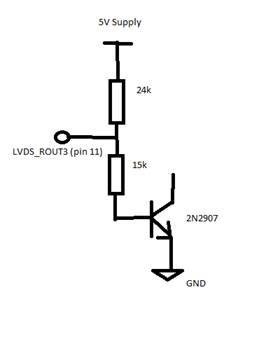
Another query about the LVDS part DS90LV032A.

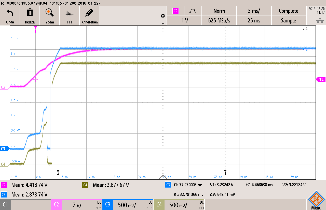
I notice that during a clean startup (5-10 milliseconds) the receiver outputs dip low for 1-2 milliseconds before reverting to default-Hi status.

Is this a characteristic of the chip design?

How consistent is it?

Any way to prevent it?

Thanks.

  • Hi,

    Please send a scope picture of the power-up window and the outputs going low.  I suspect the supply voltage has not yet reached the recommended operating range.

    When VCC = 0 the Ro output impedance is not specified.  The IIN specification shows that the inputs are Hi-Z.  I suspect the outputs will behave like diodes if the output voltage is forced above or below 0V when VCC = 0V.

    Regards,

    Lee

  • Hi Lee,

    Attached are two scopes.

                   SCR50 shows the supply rail powering up (3.3V; “C4”); C2 is the a 5V rail used for triggering the scope. The 3V3 rail power-up takes about 4 milliseconds.

    SCR51 shows the same 5V rail for triggering, and two different DS90LV032A receivers’ R0 pins. The “+” and “–“ differential inputs are not connected, but terminated with 100 ohms locally.

    We do not have any external biasing as yet.

    Ro connects to a pull-up resistor that powers the base of an NPN – when the Ro is active (low) it pulls down the base and disables the NPN. Ro is expected to be either Hi-Z or default-High during startup, allowing the pull-up to dominate.

    Thanks.

  • Hi,j

    It looks like something in the circuit is already starting to load the circuit at VDD = 500mV. 

    Can you send the schematic so we can have a better look at the components.

    Thanks and Regards,

    Lee 

  • Hello,

    Haven't heard back from you for a while. I will close this thread, but if you still need assistance, please reply to the thread and it will get open again.

    Regards,
    Yaser
  • Hi Yaser,

    Apologies for the delay.

    The load on the LVDS output is as follows. Note that in this power-up scenario the 5V is also ramping up from zero. Steady-state bias if the LVDS IC is hi-Z should be 2.4V.

    Thanks.

  • Hello,

    The behavior of output when Vcc is outside the recommended range cannot be guaranteed. So, unfortunately, I am really not sure how consistent this behavior would be. Have you tried to observe the behavior when the output is not connected to anything?

    Regards,
    Yaser
  • Hello,

    Haven't heard back from you for a while. I will close this thread, but if you still need assistance, please reply to the thread and it will get open again.

    Regards,
    Yaser
  • Hi Yaser,

    Customer have decided to change to a 5V LVDS IC rather than 3V3: probably DS90C032QML.

    There is effectively a similar large capacitor filter (100-200uF) on this rail with similar slew rate. Are we likely to still see the glitch?

    Thanks.

  • Hi Ikon,

    There shouldn't be a glitch, however, we are not sure why there was one to start with. Please try it and see how it goes. If they still see the glitch, please try to observe the behavior when the output is not connected to anything.

    Regards,
    Yaser