This thread has been locked.

If you have a related question, please click the "Ask a related question" button in the top right corner. The newly created question will be automatically linked to this question.

HD3SS3220: Connection status issue

Part Number: HD3SS3220
Other Parts Discussed in Thread: TUSB1002, TUSB1002A

Hi,

I'm having an issue with the HD3SS3220 USB controller. When reading the connection status register at address 0x09, the value returned is always 00100000 which indicates that the device is not yet attached even though it's connected to a USB 3.0 port. On power up, how long do I have to wait before being able to communicate via I2C with the device controller? according to the datasheet on page 18, it states and I quote "The HD3SS3220 local I2C interface is available for reading/writing after x clock cycles when the device is powered up". What is exactly should this x clock cycle value be? why is it that the HD3SS3220 cannot sense it's already connected.. do I have to manually set it's connection status?

Is anyone else having similar connection status issues?

regards,

Luis Gonzalez

Beckman Coulter, Inc

  • it need 100ms to read the status
  • I currently wait for 170 ms but still the status never changes from previously stated
  • does the HD3SS3220 require a driver for it to be detected?

    regards,

    Luis Gonzalez
    Beckman Coulter, Inc
  • I'm trying to read status register 0x09 from an FPGA via I2C protocol but no matter how long I wait, the status never changes from initial default state (unattached and DRP mode) even if the controller is already connected to another USB 3 port. Do I have to manually configure the controller? if so, is there a guide showing the proper procedure for detecting and initializing the state of the controller?

    thank you!

    Luis Gonzalez
    Beckman Coulter, Inc
  • Most likely issue is with non-failsafe pins cause backdrive and resulting in device not getting reset properly.

    can you check to make sure non-failsafe pins are handled properly?
  • These pins are handled accordingly.. is there a Linux or windows driver for this controller?

  • Luis

    You don't need a Linux or Window driver for HD3SS3220.

    Thanks
    David
  • David,

    How is it possible that no driver is required for the HD3SS3220. when I connect the HD3SS3220 to either a windows or Linux system with a USB3.0 port, it doesn't get recognized so how can any data transfer occur. Can you please explain to me how is it possible that no driver is required?

    thanks!

    Luis Gonzalez

  • Luis

    HD3SS3220 manages the connection and switching of the SuperSpeed USB signal between USB host/device and Type C connector base on the voltage of CC1 and CC2. It is a state machine based design, so no Window/Linux driver is needed. The USB device needs to provide Window/Linux driver if needed.

    Are you connecting to a host or a device? What is the voltage of CC1 and CC2?

    Thanks

    David

  • hi David,

    I'm connecting to a windows PC so technically a host. The HD3SS3220 is in DRP mode. Port pin is left floating and Address pint is pulled up. voltage level on CC1 and CC2 is 5V. what kind of event should I expect on the host PC to let me know that the HD3SS3220 has been recognized though?

    thanks!
    Luis
  • Luis

    Can I take a look at your schematic? CC1 and CC2 can't be 5V at the same time. You can use DIR pin to check the cable orientation.

    Thanks
    David
  • David,

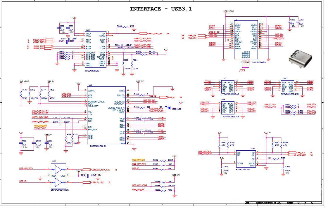
    Sorry, the 5V is only on CC1. Cable orientation is on CC1. attached is the USB section of the schematic..

    thanks!

    Luis

  • Luis

    If you are only seeing 5V on CC1, this is good. Are you only seeing 5V on CC2 when you flip the cable?

    On the schematic,

    1. Please change TX1P/N and TX2P/N cap from 0.22uF to 0.1uF
    2. Please change USB31_DRV_RXP/N cap from 0.22uF to 0.33uF
    3. Please remove cap on USB31_DRV_TXP/N
    4. Do you have cap on USB31_TXP/N?
    5. Please change R185 and R187 from 100k to 220k. Or you can replace TUSB1002 with TUSB1002A and remove these two resistors (recommend)
    6. Are you driving TUSB1002 EN high or low?
    7. For DRP, do you have an external VBUS switch?
    8. 10k instead 499k pullup on CURRENT_MODE pin
    9. 200k pullup on INT_N_OUR3 pin
    10. 200kpullup on ID pin

    If after making these changes we are still not seeing the connection, please probe TX and RX on both side of TUSB1002 and HD3SS3220. We should first see LFPS signal, which is a clock signal.

    If we see LFPS, then the connection is correct, then this could be a signal integrity issue, and we need to change the EQ and CFG setting of TUSB1002.

    Thanks
    David
  • Hi David,

    I'm currently in the process of making your recommended changes to the circuit and will update you as soon as possible. Once the link is up, what event will the operating system (windows or Linux) do though to indicate me that It has recognized the port and its attached, do you know? Normally, when you connect a USB 2.0 device to the PC (host), the operating system will try to look and load a driver for the newly attached device. Will something similar occur in this situation once the link has been attached correctly?

    Thank you so much!

    Luis Gonzalez

    Beckman Coulter, Inc
  • David,

    to answer your three questions,
    Q1. Do you have cap on USB31_TXP/N?
    A. Yes, they are 0.1uF 16V X7R
    Q2. Are you driving TUSB1002 EN high or low?
    A. High
    Q3. For DRP, do you have an external VBUS switch?
    A. Yes

    thanks!
    Luis Gonzalez
    Beckman Coulter, Inc
  • Luis

    Enumerating USB3.0 devices has some differences compared to USB 2.0, but the general principle will be the same.

    Once you made the changes, I would probe TX and RX on both side of TUSB1002 and HD3SS3220. We should first see LFPS signal, which is a clock signal.

    If we see LFPS, then the connection is correct, then this could be a signal integrity issue, and we need to change the EQ and CFG setting of TUSB1002.

    Thanks
    David
  • Luis:
    any update?
  • Brian,

    I'm currently in the process of making changes to the hardware as per David's recommendations. Unfortunately, I didn't have all the parts at hand so I had to order and I just received. I should have an update by tomorrow..

    thank you!

    Luis

  • David,

    I made all the resistor and cap changes except for two of them. The 499k pull up ensures that the current mode is set to 1.5A correct so why put a 10k which will change the current mode to be 3A, is that much current require for it to work properly?
    Also, I couldn't change the cap on USB31_DRV_RXP/N because the ones I ordered did not arrive along with the other parts but will make the change as soon as it arrives.
    Looking at the documentation for the TUSB1002 redriver, I noticed that on page 19 table 4 they have similar recommendations for the AC coupling like the ones you suggested. So instead of completely removing the cap on USB31_DRV_TXP/N, I replaced it with a 0.1uF. That shouldn't be a problem correct?
    I'm about to probe TX and RX on TUSB1002 and HD3SS3220 and let you know if I see the Low Frequency Periodic Signal...

    Thanks!
    Luis
  • Luis

    You need to remove the caps and short across for USB31_DRV_TXP/N since the signal is already biased on the other side of HD3SS3220.

    Thanks
    David
  • David,

    Ok I see. I'll replace the caps with shorts then. How about the 10k pull up, is it necessary to have a current mode of 3A?

    Thanks!
    Luis
  • David,

    How big of an LFPS burst should I see on the scope in terms of voltage level? will it be less than 1Vpp or higher?

    Thanks!
    Luis
  • Luis

    LFPS is a clock waveform with minimum of 800mV and max of 1.2V amplitude.

    Thanks
    David
  • Hi David,

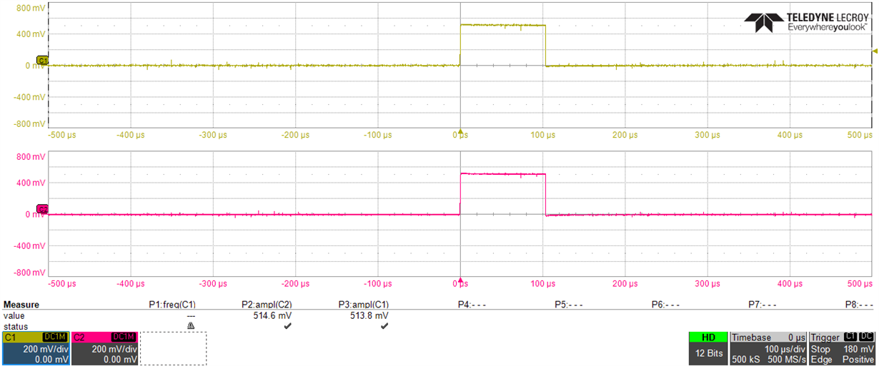
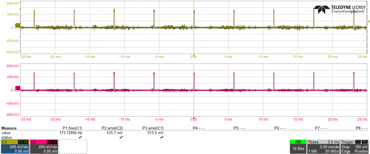
    Unfortunately, I'm still waiting for the 330 nF caps and also for some 0 Ohm resistors to be able to short the USB31_DRV_TXP/N lines. However, I decided to probe the TX1P/N lines on the HD3SS3220 and to my surprise I'm getting an output. The output I'm getting appears to be a common mode signal though. The output signal is about 515mV and repeats approximately every 5.76 ms or so. Please take a look at the attached oscilloscope output.

    Thanks!

    Luis

  • Luis

    This looks like far-end RX detection after the U2/U3 state, with HD3SS3220 being a switch only, this looks coming from the host.

    Thanks
    David
  • David,

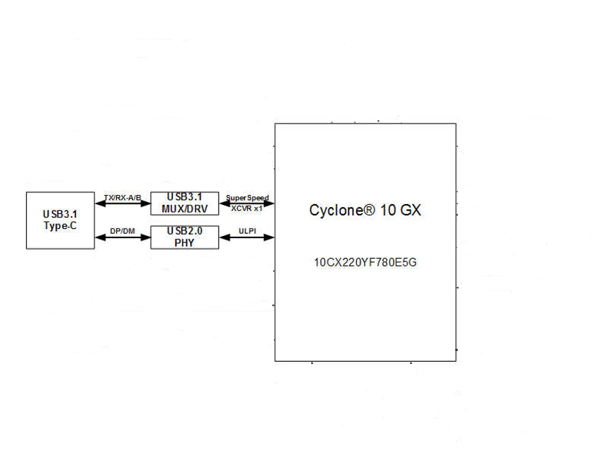
    I'm new to the USB 3.1 protocol as probably many other people out there might be so when you say that the output looks like a far-end-RX detection after the U2/U3 state coming from the host, it kind of confuses me a little. By the way, I'm using an Intel Cyclone 10 GX dev kit and the way the USB 3.1 Type C is all connected is as follows:

    The USB31_TXP/N and USB31_RXP/N lines going into the TUSB1002 redriver come directly from the FPGA. Currently in the FPGA, I have a state machine in which I poke via i2c protocol the connection status register at address 0x09 on HD3SS3220 to verify the state of the DRP controller and see if it's already attached and in DFP or UFP mode so I can begin transmitting a specific test pattern which is not close to what I captured on the oscilloscope. I'm not using the USB 2.0 interface at all by the way.

    If you don't mind, can you please elaborate a little more on the far-end RX detection and U2/U3 states?

    Thanks!

    Luis

  • Luis

    The Receiver Detection circuit is implemented as part of a Transmitter and will correctly detect whether a load impedance equivalent to a DC impedance (min 18ohm and max 30ohm) is present. The Rx detection operates on the principle of the RC time constant of the circuit.
    This time constant changes based on the presence of the receiver termination. Once detecting the link partner at the other end. we then moves to Polling.LFPS as part of the link training.

    TUSB1002A does RX detection on both of its TX1 and TX2. When TX1 and TX2 detect the receiver termination of the link partner, it will enable its own RX termination on RX1 and RX2 so both TUSB1002A and link partner can complete the detection and start the link training.

    There are four operational link states, U0, U1, U2, and U3. U0 is the normal state where an Enhanced SuperSpeed link is enabled. U1 is low power link state where no packet transfer is carried out and the Enhanced SuperSpeed link connectivity can be disabled to allow opportunities for saving the link power. U2 is also a low power link state. Compared with U1, U2 allows for further power saving opportunities with a penalty of increased exit latency. U3 is a link suspend state where aggressive power saving opportunities are possible.

    Thanks
    David
  • Hi David,

    Thank you for that explanation. So based on the fact that it is a possibility that the far-end Rx termination detect process is in progress, what do you think could be happening that the link training state is not yet occurring?
    If after placing shorts on the USB31_DRV_TXP/N lines and changing the 0.22uF caps to 0.33uF on the USB31_DRV_RXP/N lines, the HD3SS3220 is still not able to establish a successful link state, what else can be done hardware wise to resolve the issue?

    thanks
    Luis
  • Luis

    I would resolve the cap first so you will have the proper bias voltage.

    The fact that far-end RX termination detect process in ongoing indicates TUSB1002A is not seeing the RX termination, either in the host or the FPGA RX. So you have to make sure host or the FPGA turns on their RX termination.

    Thanks
    David
  • David,

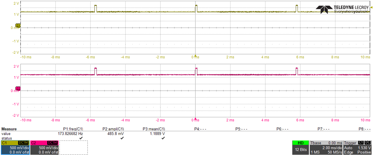
    After taking care of the caps on the USB31_DRV_TXP/N lines by replacing them with shorts, the output now appears to be DC biased by about 1.2V. Please see screenshot below:

    By the way, the measurement was taken with a single-ended probe for each line USB31_DRV_TXP and USB31_DRV_TXN respectively. It appears the far-end-RX termination process is still ongoing. The Tx/Rx settings on the FPGA for USB31_TXP/N and USB31_TXP/N are as follows:

    Rx settings:

    On-chip termination for transceiver Rx pin : 100 ohms

    Receiver High Data Rate Mode Equalizer : On

    Receiver High Gain Mode Equalizer DC Gain Control : 0

    VCCR_GXB/VCCT_GXB Voltage : 1.0V

    Receiver Variable Gain Amplifier Voltage Swing Select : 2

    Receiver High Data Rate Mode Equalizer AC Gain Control : 3

    Tx settings:

    On-chip termination for transceiver Tx pin : 100 ohms

    Transmitter link type : chip-to-chip

    Transmitter output swing level : 1000mV

    Transmitter High Speed Compensation : On

    Transmitter Pre-Emphasis 1st Pre Tap : 0

    Transmitter Pre-Emphasis 1st Post Tap : -3

    Transmitter Pre-Emphasis 2nd Pre Tap : 0

    Transmitter Pre-Emphasis 2nd Post Tap : -3

    One last thing to note is that I still have yet to replace the 0.22uF caps on USB31_DRV_RXP/N with 0.33uF but I'm not sure if that will make that big of a difference, will it?

    Thanks!

    Luis

  • Luis

    Is the termination on both FPGA TX and RX are enabled?

    With 0.22uF on USB31_DRV_RXP/N and assume 0.1uF on the corresponding TX, you total capacitance would be 0.6875uF, below the spec requirement of 0.75uF.

    With 0.33uF, you would then 0.76uF, right at the spec limit.

    Thanks
    David
  • Hi David,

    Yes, termination of both Tx/Rx lines from FPGA are enabled. Wouldn't the total series capacitance equal to 0.06875uF from the 0.22uF and assumed 0.1uF? by replacing the 0.22uF with the 0.33uF, the total series resistance would then be 0.76nF and not 0.76uF. is the spec limit in micro Farads (uF) or nano Farads (nF)? because if it's in micro Farads then I would still be way below the spec limit.

    Can you please confirm if the spec limit you just mentioned is in micro Farads or nano Farads?

    Thanks!

    Luis

  • Luis

    Yes, this is a typo on my part. It should be 68.75nF with 0.22uF cap, below 75nF. With 0.33uF, it is 78nF, right above the spec limit.

    Thanks
    David
  • David,

    Thank you so much for the confirmation..

    Luis
  • David,

    Finally got the remaining parts, zero ohm resistors and 0.33uF caps. I replaced the caps on the USB31_DRV_TXP/N lines with the zero ohm resistors as you recommended and the 0.22uF caps on the USB31_DRV_RXP/N lines with the 0.33uF caps. However, as can be seen from the screenshot below, the output at USB31_DRV_TXP/N looks exactly the same as my last screenshot post in which the Far-end-Rx termination detection is still ongoing.


    All caps and pull ups have been changed as you recommended except for the 499K Ohm pull up on the CURRENT_MODE pin since a mid current level of 1.5A should be good enough. Termination of Tx/Rx on the FPGA are enabled and set accordingly.

    What else do you think could be happening here that's preventing the HD3SS3220 DRP controller from starting the link training process?

    The host to which the HD3SS3220 DRP controller is connecting to via the USB31 connector is a Q7 development board (SOM DB3520) which has USB3.0 ports. The interfacing cable being used to connect the two is a USB 3.1 A/M Type C Gen 1 cable from Qualtek electronics (https://www.alliedelec.com/product/qualtek-electronics-corp-/3023039-01m/70728014/).

    Is the HD3SS3220 DRP controller USB 3.0 backwards compatible?

    Thank  you!

    Luis

  • Luis

    What is being connected at the Type C connector?


    If you probe the CTXP/N2 and CTX1P/N, are you also seeing the far-end detect?

    Thanks
    David

  • David,

    I'm connecting the Type C connector on the Cyclone 10 GX dev kit to one of the USB 3.0 ports on the Q7 development board (SOM-DB3520) that I had mentioned in my previous post. When I probe CTX1P/N, I'm seeing the same thing but not when I probe CTX2P/N.

    thanks!

    Luis

  • Luis

    The factor that you are still detection pulse means RX has not enabled its termination. Once RX termination has been detected, you should then see the LFPS. Can you take a multi-meter and measure the RX pin to GND and see what is the resistance?

    Does the FPGA also implement the far-end RX detection to detect TUSB1002 RX termination?


    Thanks
    David

  • David,

    The measured resistance between USB31_DRV_RXP and GND is 9.302M Ohms. The FPGA does not implement the far-end-Rx termination detection. however, the Tx/Rx terminations are enabled on the FPGA.

    thanks!

    Luis

  • Luis

    The FPGA has to implement the far-end RX termination detection in its TX. Otherwise, you will not detect the connection event. This is the reason why we are stuck in RX detect state.

    Thanks
    David
  • David,

    My apologies, I forgot to mention that I do instantiate a transceiver IP core in the FPGA. Shouldn't this core be doing the far-end receive detection or do I have to create additional logic to be able to do the far-end receive detection?

    thank you!

    Luis
  • David,

    Based on what you're telling me and the more I think about it. I think it might be necessary to develop a full blown USB device controller core to handle the DRP controller because I was under the impression from one of our previous conversations that the DRP controller had its own state machine logic inside to handle the connectivity and be able to present itself to the HOST PC as a device controller so that the enumeration can then be taken care of by the HOST operating system. Is that still the case or no and if not, do you think developing a full blown USB device controller on the FPGA would be the best way to go then?

    thanks!

    Luis

  • Luis

    You also need a USB compliant PHY to handle the connectivity. HD3SS3220 is a DRP controller, it handles the connection of USB SuperSpeed signal path, but it is not a device controller, full enumeration has to be handled by the FPGA.

    Thanks
    David
  • David,

    So a USB device controller core with a fully compliant phy transceiver core together would resolve this connectivity issue then, correct?

    thanks!
    Luis
  • Luis

    Yes, please make sure the device controller IP is also fully compliant to both USB3 and USB2. Depending on the data rate requirement, the IP needs to be either Gen 2 10G or Gen 1 5G compliant.

    Thanks
    David
  • David,

    Ok, I see. I'll have to develop that but USB 2.0 support is a must as well?

    Thanks!
    Luis
  • Luis

    Yes, this is to maintain backward compatibility if USB3 fails.

    Thanks
    David
  • David,

    Ok got it. Makes sense. I've developed USB 2.0 compliant cores before but this will the first for USB 3.1. Any recommendations on where I might be able to get more info on the USB 3.1 spec. I imagine it's got to be very similar to USB2 in the sense that it makes use of EndPoints, Tokens and so forth, correct?
    I guess the circuit changes made did get the DRP controller to at least begin to talk because I was not seeing anything before. Is there any additional circuit changes you think should be made or the ones already done are good enough?

    thanks!
    Luis
  • Luis

    Mindshare has a good tutorial on USB3: www.mindshare.com/.../USB 3.0 Technology.pdf. For more detailed answer, I would then refer to USB3.1 spec.

    For IP, please refer to Cadence or Synopsys
    ip.cadence.com/.../usb-3-0-controller
    www.synopsys.com/.../ipdir.php

    Thanks
    David
  • David,

    Thank you so much for your assistance and recommendations. I really appreciate it. I now know what's remaining to make the controller go pass the far-end-rx detection state.

    I'm guessing no more additional circuit changes need to be made?

    thanks!
    Luis