Part Number: PCA9306
HI,
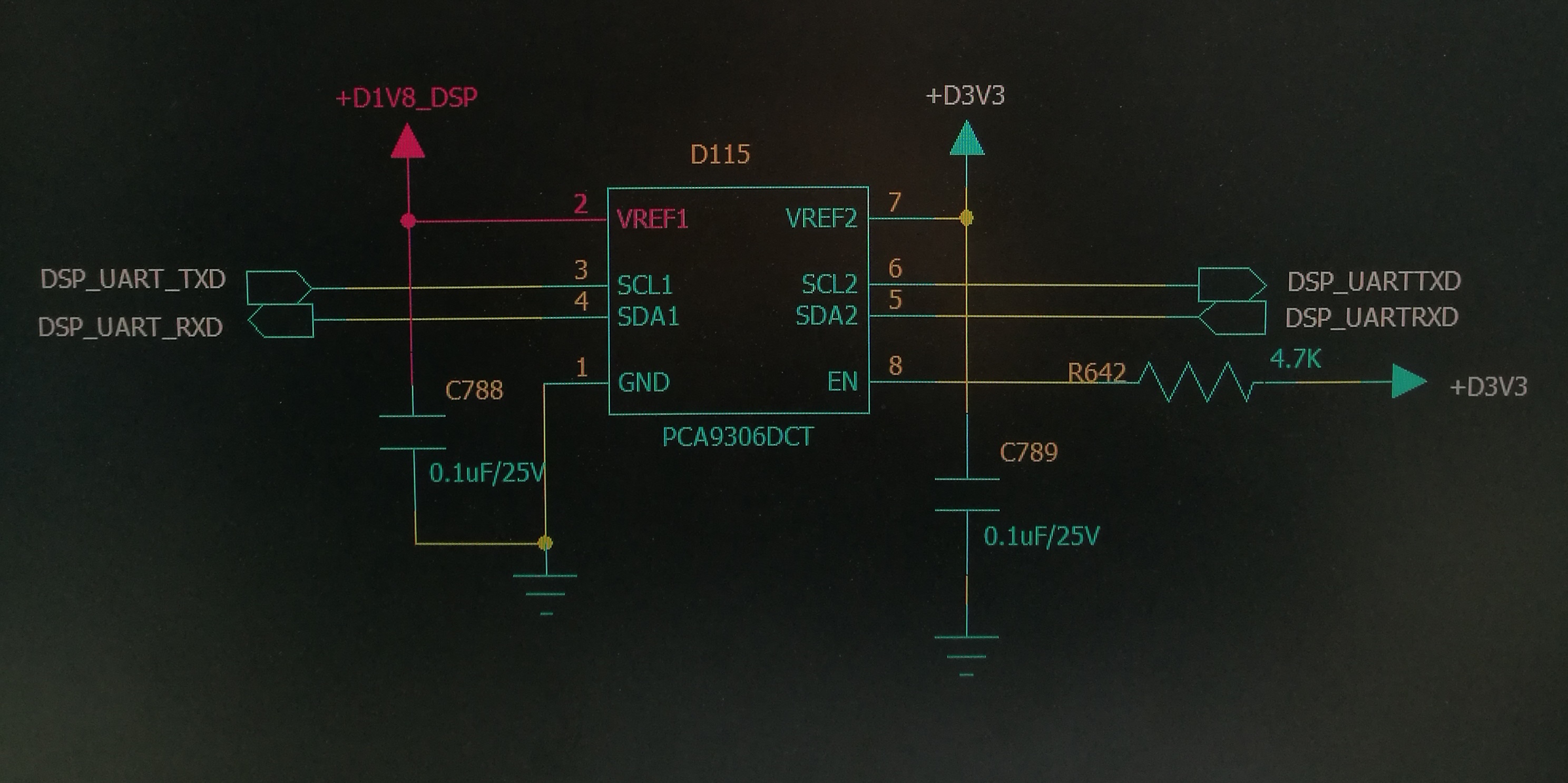
We have tied EN to 3.3V with a pull-up resistor of 4.7k ohm, and the vref2 directly to 3.3V, the 3.3V is always enabled.
VREF1 is tied to 1.8V which is powered up and down as needed.
I learned in the forum that this design is not reliable.
Is there any way to reduce the risk with minimal changes?
Is there a chip that can replace it without changing the package and design?
Sincerely,
Li