This thread has been locked.

If you have a related question, please click the "Ask a related question" button in the top right corner. The newly created question will be automatically linked to this question.

SN75LVDS83B: Transmitter output clock problem

Part Number: SN75LVDS83B

Hi All. I have FT810 that works with display 320x240 pixels with RGB interface (G057QN01 V2 display).

I am trying to drive an new LCD which uses an LVDS interface. Display is next: G084SN05 V9 with 800x600 pixels. 
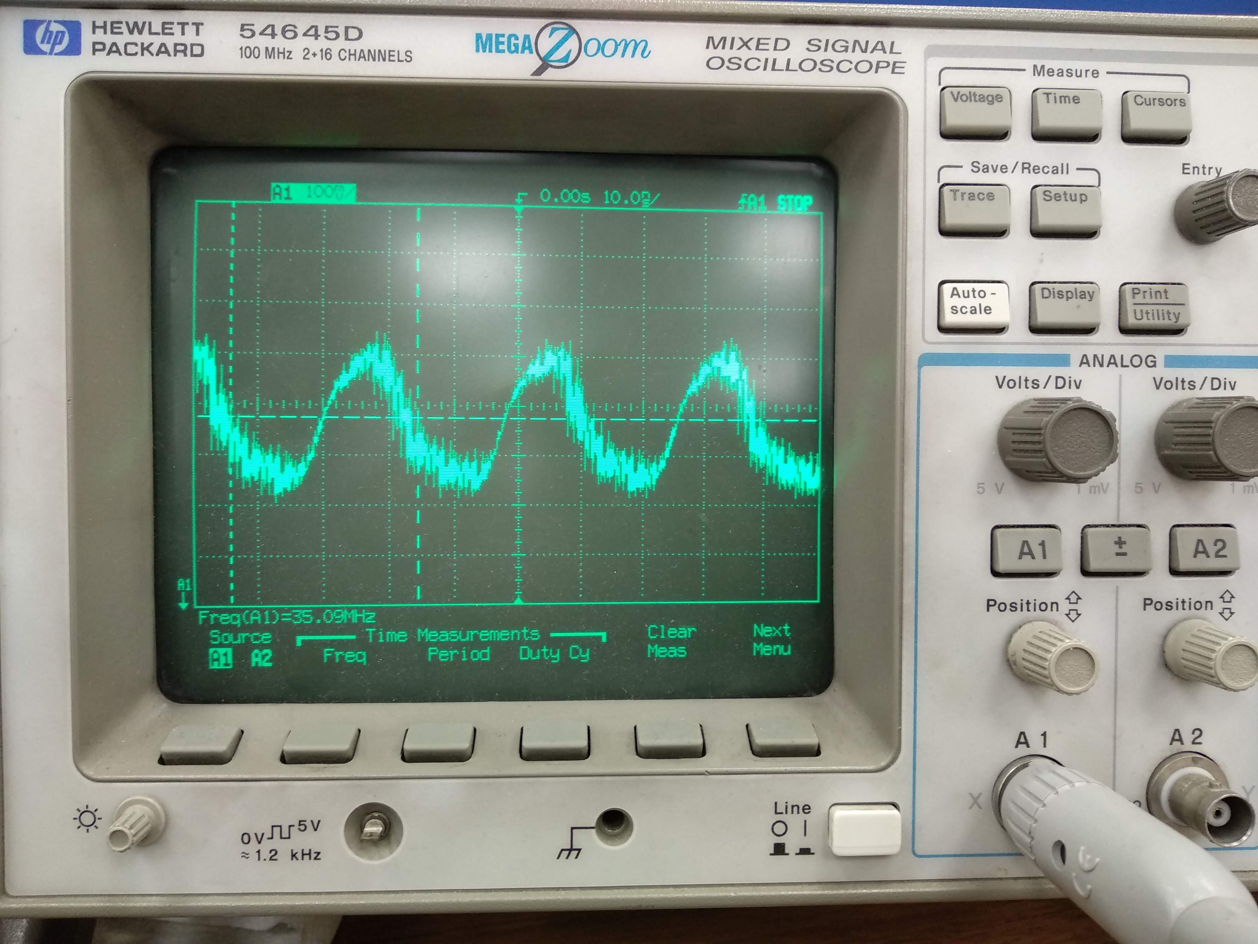
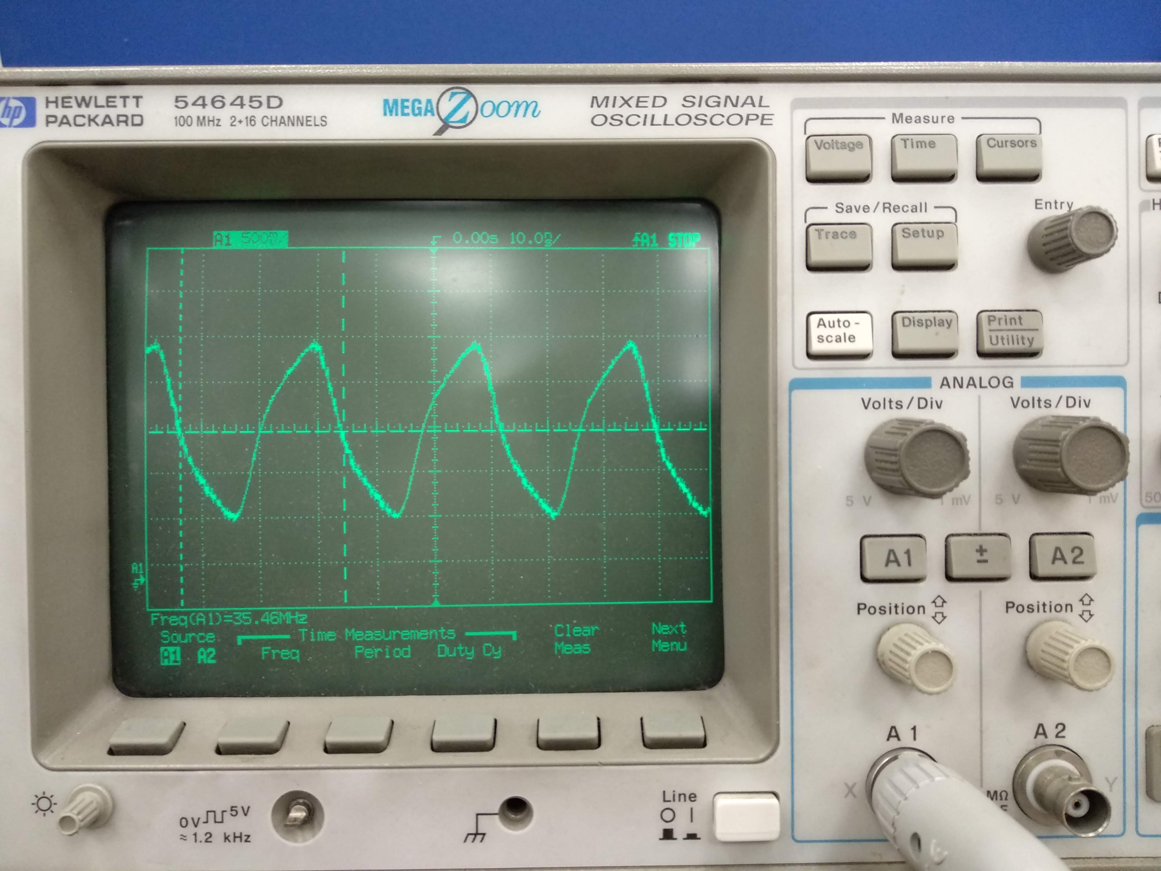
i am using an SN75LVDS83B FlatLink Transmitter for conversion from RGB to LVDS interface. But display is not turned on, back light is not turned on. After some checking, i found that output clock signal from SN75LVDS83B to LCD have a noise, input clock  is OK. Is that noise is acceptable or it can be reason of LCD is not turned on? I do not understand why output clock of transmitter have such noise.

Input clock to transmitter:

Output clock from transmitter to LCD:

  • Hi Yury,

    Have you checked for any issues with your display? Even with a noisy clock I would expect to see something on the display rather than nothing at all.

    Also, are you following the the power up sequence on page 20 of the datasheet?

    Regards,
    I.K.
  • Thank you for reply. Yes all started to work. The problem was at backlight cable. But i am very surprise that LCD is working with such noisy signal.
    As i understand, power up sequence from datasheet is not necessary condition. From application I can control only signal data and Back light on/off pin. All other pins are hardware fixed by HW engineer: VDD, VCC, Back light dimming and are activated in same time during power up.
  • Hi Yury,

    Correct, the sequence is not required but is just recommended for some systems. So is there no issue with your display now? The noise may be due to the PCB layout. You can reference this application note for future designs to reduce noise: www.ti.com/.../snla302.pdf

    Regards,
    I.K.