This thread has been locked.

If you have a related question, please click the "Ask a related question" button in the top right corner. The newly created question will be automatically linked to this question.

SN65DPHY440SS: connecting data lanes of the camera 0..1..2..3 to 2..3..0..1 input of the sn65dphy440ss

Part Number: SN65DPHY440SS

Hello Team,

I have a question which is very important for my design.

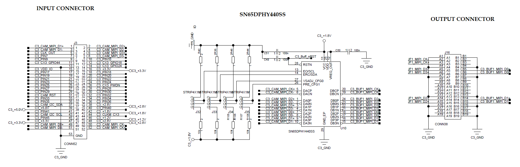
for a better routing reason, it would be great to connect the four lanes of any camera to the input of the sn65dphy440ss device with a different sequence.

Let's say, the connector from which I get the four lanes of a camera (0..1..2..3) are connected to the input of the sn65dphy440ss device to the following ports: 2..3..0..1, while the clock lane has not been changed of course.

i try to summarize here below the connection:

Camera   Connector        TI Buffer In        TI Buffer Out                  Receiver

Lane0 --------------------------Lane2_in------Lane2_out------------------Lane0

Lane1 --------------------------Lane3_in------Lane3_out------------------Lane1

Lane2 --------------------------Lane0_in------Lane0_out------------------Lane2

Lane3 --------------------------Lane1_in------Lane1_out------------------Lane3

LaneClk------------------------LaneCk_in----LaneCk_out----------------LaneClk

From the datasheet I didn't understand whether the four data inputs of the sn65dphy440ss device are equivalent or not.

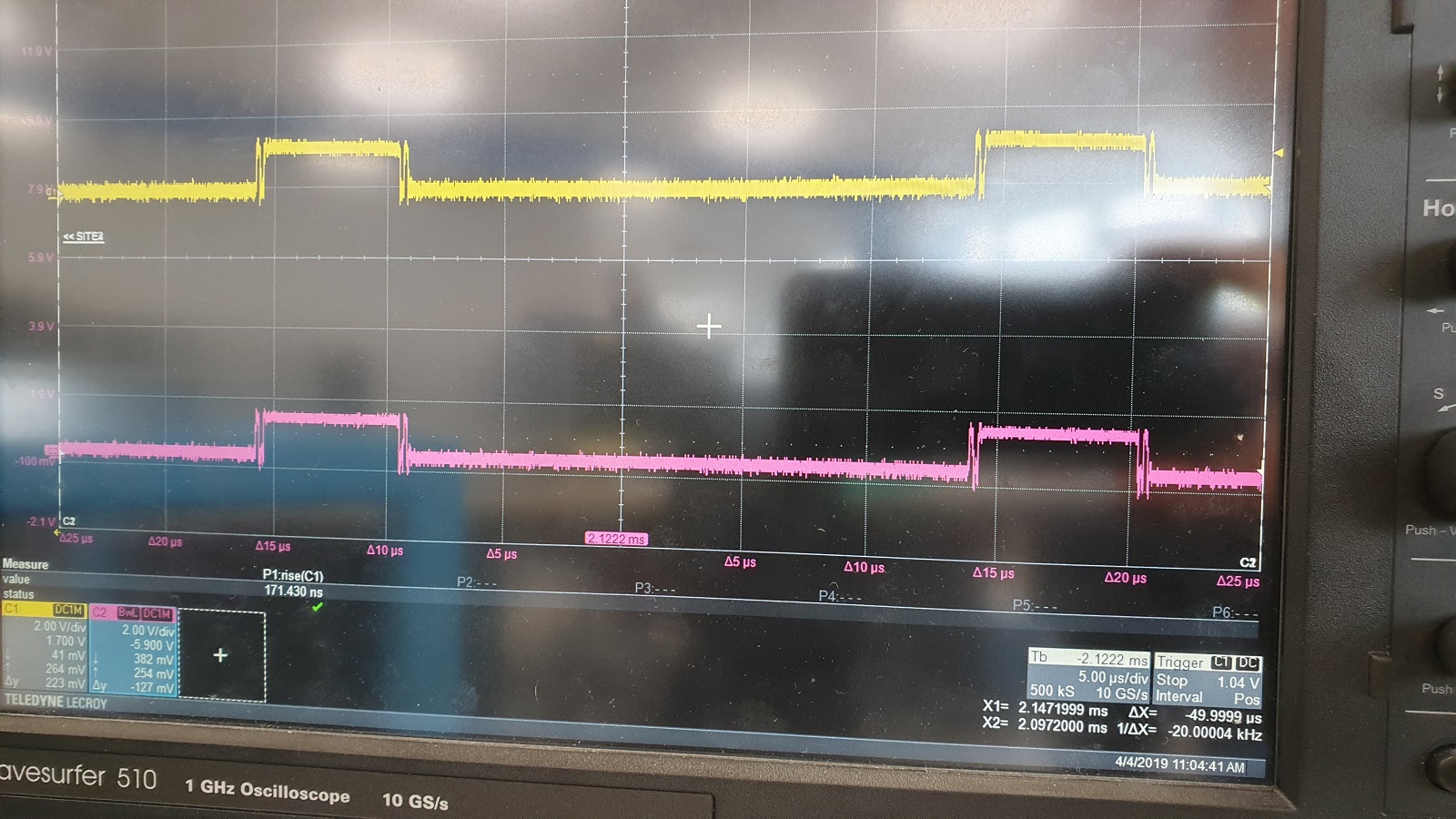
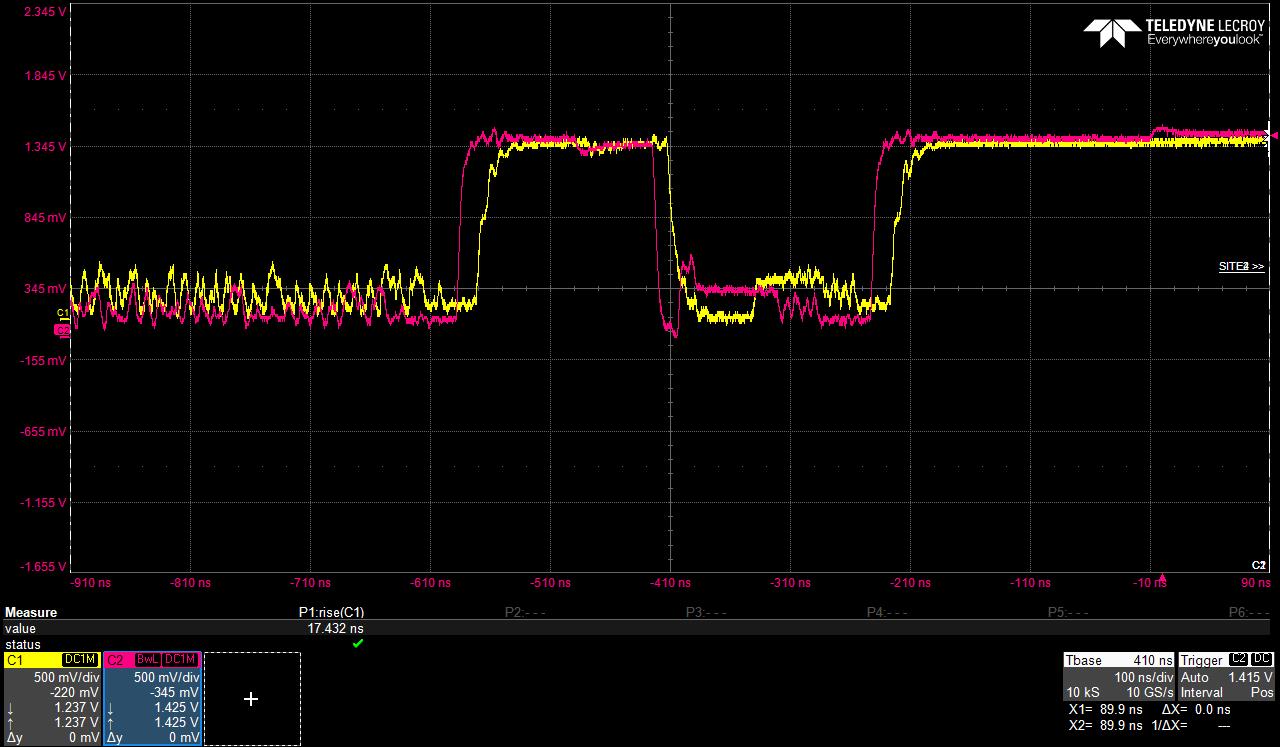
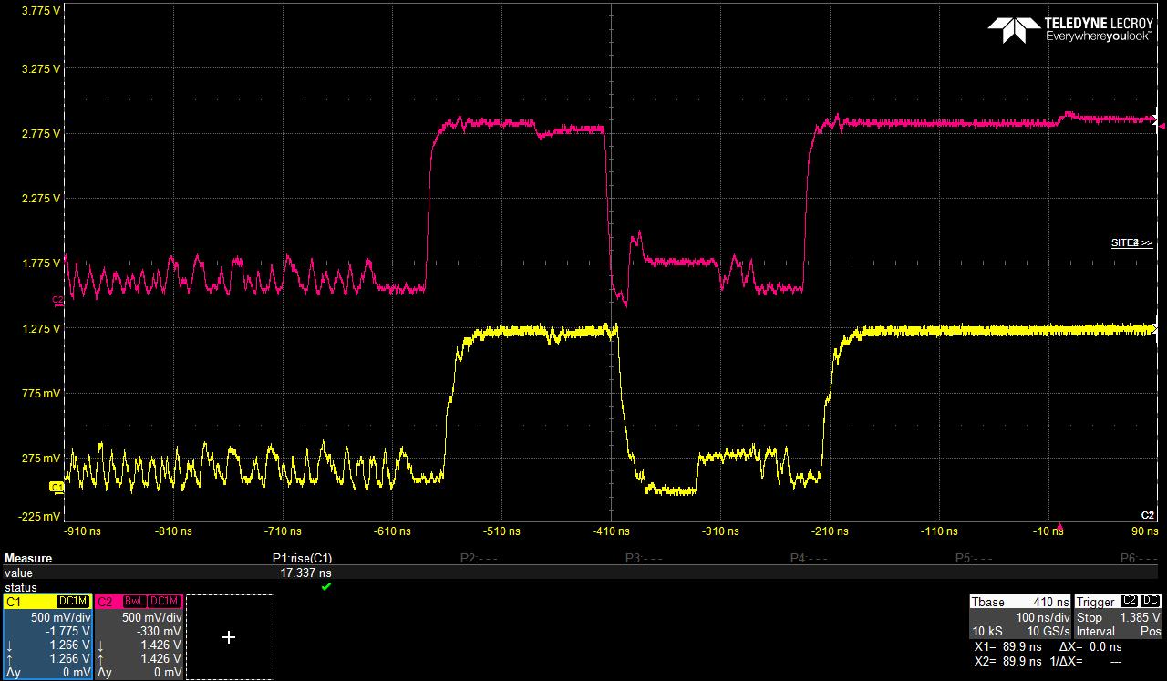
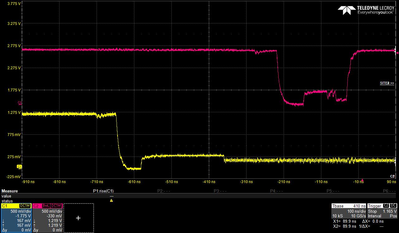
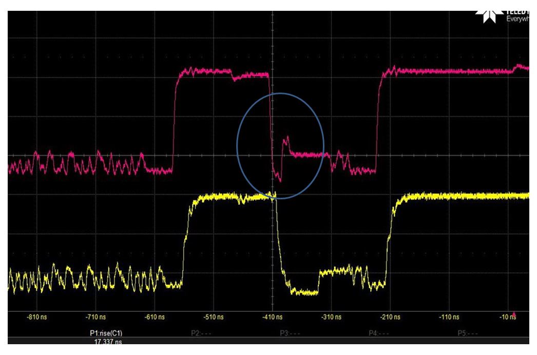
Now I have designed a temporary engineering board with the above connection.

The camera used at this moment has only data0 and data 1 outputs.

these outputs are using the lane 2 and lane3, as above shown.

But unfortunately I cant get the image from the receiver.

If I connect the receiver directly to the camera, everything is working.

I hope my question is clear.

Many thanks in advance for your support

Stefano

  • Stefano

    For CSI-2, DPHY440SS does not care about the lane ordering.

    For DSI and if back channel is supported, then lane 0 has to be lane 0 because lane 0 is the only lane that supports backchannel.

    Thanks
    David
  • Dear David,

    thanks for your prompt reply.

    So, do you mean that whatever is the channel assignment, the only requirement is that the channel 0 must be assigned to an active channel?

    In my situation, since I am basically using channels 2 and 3 of the device , while the channels 0 and 1 inputs are stuck to GND, it means it can't work ?

    So maybe that's the reason why my Engineering board isn't working?

    many thanks again,

    Stefano
  • Stefano

    If you don't need back channel, then you don't need to use channel 0. Does the camera or receiver require back channel support?

    Thanks
    David
  • Sorry David,

    I misunderstood what you said before.

    I'm actually not aware about backchannel in Mipi-CSI2.

    I only know that I have a camera with (in this case) 2 lanes and I need a buffer to re-generate the signal after passing trough a couple of connectors.
    These 2 lanes (0 and 1) are connected to the input lanes 2 and 3 of the sn65dphy440ss device, while the input 0 and 1 stuck to GND.

    the outputs 2 and 3 are then connected to my receiver.

    The boards isn't working, but if I bypass the sn65dphy440ss device, I can correctly receive the data.

    That's why I was wondering if the 4 lanes are really identical.

    I'm not expert on the CSI2 protocol, but as far as I know it automatically recognize the LP vs HS status.
    I was wondering if this status is checked only on the lane 0, if somehow the lane 0 is the one "triggering" the whole device.

    I'm confused. I have checked also all the power supply pins and everything looks ok.

    any idea baout how to proceed?

    thanks again

    Stefano
  • Stefano

    CSI-2 does not have a back channel path. Because of this, there is no requirement on lane ordering, so connecting to input lane 2 and 3 should be OK.

    Are you seeing the data on the output lane 2 and 3? If you are seeing data, then you may need to change the setting of VSADJ_CFG0, PRE_CFG1, EQ, and ERC setting.

    Can I take a look at your schematic?

    Thanks
    David
  • I didn't  check the output yes because today I didn't  get the oscilloscope, but tomorrow I will do for sure.

    Regarding the register, in my schematic I used jumpers for having the possibility to select high/middle/low voltage as input of EO/ERC/CFG0/CFG1 pins.

    I am using the middle voltage for loading at the startup a "compromise" as default values..

    keep in consideration that I have few inch of traces with 100 ohm impedance. So I think we dont need a big emphasis.

    below you can see the schematic: at the input connector we have the CSI2 signals from the camera.

    then we have the repeater, with the jumpers above mentioned and inputs 01 and 23 swapped.

    when we have the output connector where the receiver is connected.

    What I have already checked is the power supply at 1.8V and the generated voltage at the VREG_OUT/VDD pins which is at 1.2V

    we have a big project which depends on this buffer, so I really need to make it working.

    any idea is welcome

    thanks again

    stefano

  • Stefano

    You may need to change the 100nF on RESETn to 200nF to make sure the DPHY440SS is being reset properly.

    The CCI does not go through the DPHY440SS, how do you connect the CCI bus?

    Thanks
    David
  • Dear David,

    I will put 200nF as suggested.

    about the CCI, what do you mean ? the I2C interface?

    If you mean the I2C interface I have a connector (not shown in the previous screenshot) which can be used to send commands to the DPHY440SS device.
    But I didn't use this interface yes because, as far as I have understood, the default values at the startup can be loaded/selected just using the resistor network by choosing Vhigh, Vmiddle, Vlow.
    Am I correct?

    Rgds,
    Stefano
  • Stefano

    CCI is camera control interface, CCI does not go through DPHY440SS, it connects directly between the CSI master and slave. It is a subset of the I2C protocol, a bidirectional, two-wire interface that master may use to configure and control cameras.

    I see on the input connector you have I2C connection, but not sure how the master is controlling the camera.

    Thanks
    David
  • Well, now I understand.


    The CCI comes from another connector not shown in this schematic, where also the receiver (which is the master) is connected.

    These signals are sent straight to the connector on the left, where the camera sensor is connected.

    The camera is correctly initialized, in fact, if i bypass the buffer i can correctly see the video.

    Tomorrow i will put 200nF on the reset and try different combination of the input voltage values.

    If needed i will connect an I2C and read the values of the internal registers.

    I will also check with the scope if the output of the buffer follows the input.

    I will give you an update by tomorrow.

    Many thanks

    Stefano
  • Dear David,

    today I have checked the register data.
    from address 0 to 7 we have the default data, as expected: {0x20, 0x30, 0x30, 0x31, 0x59, 0x48,0x50, 0x44}

    from address 0x08 onward I see the following data:

    Standard CSR Register (0x08) 02
    Standard CSR Register (0x09) 0F
    Standard CSR Register (0x0A) 12
    Standard CSR Register (0x0B) AA
    Standard CSR Register (0x0C) 00
    Standard CSR Register (0x0D) 00
    Standard CSR Register (0x0E) 11
    Standard CSR Register (0x0F) 00
    Standard CSR Register (0x10) FF
    Standard CSR Register (0x11) FF

    I dont see big issues...

    do you see anything wrong ?

    best regards

    Stefano
  • Stefano

    Do you see data on the output of DPHY440SS if you probe with a scope?

    You may need to tweak register 0x09h and 0x0Eh. Currently, EQ is set to max for both clock and data, you may want to change EQ to see if you get a better performance. Register 0x0Eh sets the transmitter voltage swing and pre-emphasis level. The current pre-emphasis level is 0dB, you may want to increase it to see if you get a better performance.

    Thanks
    David
  • Hello David,

    here below pic from the oscilloscope on one of the lanes:

    I dont know what these signals are, but I can clearly see that the output (purple) follows the inpit (yellow).

    tomorrow I will try to modify also the registers value: today I had an hard time to make the I2C working starting from a FTDI device, but at the end I got it!

    if meanwhile this picture gives you some idea, please let me know.

    as additional info, I saw the same signal when using the board without buffer (direct connection), so I am quite sure the csi2 signals look like that.

    many thanks for your support 

    Stefano

  • Hello David,

    today I made several trials.

    I have added 100nf on the existing 100nf capacitor for the reset pin.

    I have programmed registers 0x09 and 0x0E as suggested (and also read back to check the programmed values).

    But I still can't  get the device working...

    I have some screenshot from the scope:

    due to the missing differential probe I wasnt able to get a clear signal, but it should be enough for some understanding.

    img1 - data0P_in and related output overlapped

    img2 - data0P_in and related output not overlapped

    img3 - data0P and clockP outputs

    img4 - clockP output better zoom and time scale

    any idea ?

    many thanks again and best regards

    Stefano

  • Stefano

    Looking at the waveform, one of question is the HS Zero time as circled in the picture below.

    Per the MIPI DPHY spec, the THS-PREPARE + THS-ZERO is minimum of 145ns + 10UI, and THS-PREPARE minimum is 40ns + 4UI, and maximum is 85ns + 6UI. Even if I take the minimum of THS_PREPARE + THS-ZERO and subtract max THS-PREPARE from it, the circled area seems to be less than the THS-ZERO. You should able to change the value in the camera register.

    The second thing to check is the setup and hold time as shown in Figure 2 and Table 6.7 of the DPHY440SS datasheet and make sure there is no timing violation.

    Thanks

    David 

  • Many thanks,

    I will check it once back in office and Ill let you know.

    Have a nice weekend,

    Stefano

  • Stefano

    Do you have an update on this one?

    Thanks
    David
  • Stefano

    I will mark this thread as resolved and close it. You can re-open the thread when you have an update.

    Thanks
    David
  • Dear David,

    I have forwarded your feeedback to the manufacturer of the MIPI camera and I am waiting for his feedback.

    He is asking for a sample of our boards to verify and find out the reason of the malfunction (it might be the one you mentioned in your email).

    So the issue is still open but it could take a couple of weeks before getting a feedback from the camera manufacturer company.

    Ill be back as soon I get their feedback.

    many thanks and best regards

    Stefano
  • Stefano

    Thanks for the update. I will close this thread for now and you can always re-open it when you reply to this thread or create a new one with the update information.

    David