This thread has been locked.

If you have a related question, please click the "Ask a related question" button in the top right corner. The newly created question will be automatically linked to this question.

SN75DP130: DP130 two/one lane fail issue

Part Number: SN75DP130
Other Parts Discussed in Thread: HD3SS460

Hello

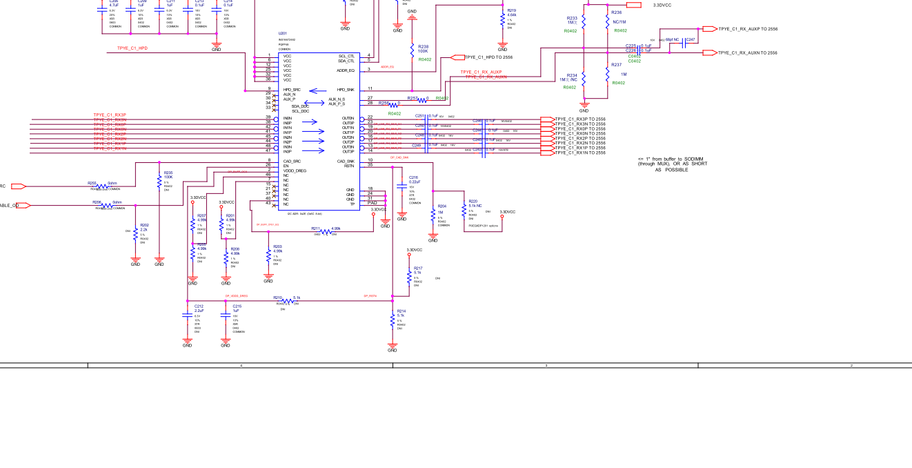
             The topology is NB-> typec connector -> Mux -> DP130 -> Monitor. If NB output four lane DP, the monitor will be light up normally. But if NB output two lane or one lane DP, monitor fail to light via DP130. 

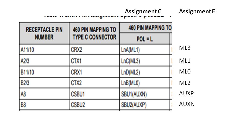
              After bypass DP130, Customer use Google NB output 2 lane and 1 lane DP, the monitor will light up normally. If use Astro VG-870 (DP to Type C cable Pin assignment E), the monitor still light up normally.

              Why two lane and one lane not light up monitor via DP130? Thank you. 

Google NB(Chrome book)

1366x768@60Hz

Astro VG-870 (DP to Type C cable Pin assignment E)
800x600@75Hz(HBR 1 lane)

BR

Patrick

  • Patrick

    Is this the same issue that you have submitted before?

    For 2 lanes, only DP0 and DP1 are used, and for 1 lane, only DP0 is used, are they correctly doing the lane assignment for the 2 lane and 1 lane? But the lane switching are handled by the mux and Scalar. DP130 does not handle lane switching.

    Does Assignment C or Assignment D work?

    If 4 lane works, but 2 lane or 1 lane does not work, I don't think this is a squelch or signal integrity issue.

    Thanks
    David
  • Hello David

    Yes. But customer bypass DP130 while at 2 lane and 1 lane then monitor light up. So it should not related to lane switching due to DP130 already bypass, right?

    Another question, if DP0+ input to IN- pin of DP130, DP- input to IN+ pin of DP130, but output will also OUT- pin output to DP0+, OUT+ pin output to DP- simultaneously as above DP130 schematics. If do polarity swapping on DP130 input/output pin, has any issue while 2 lane or 1 lane? Thank you.

    BR
    Patrick
  • Patrick

    When bypassing DP130, are they also bypassing the 10G Mux? I don't have the datasheet for the 10G Mux so I can't comment on how the Mux handles the Assignment E lane mapping.

    If the polarity matches between input and output, then this is not an issue.

    It will be best if they have the AUX monitor tool so we can see the entire link training sequence.

    My expectation is that if 4 lane is working, then 2 lane or 1 lane should work as long as the line ordering is correct.

    Thanks
    David
  • Hello David

    Customer use RTS5450 for 10G mux. Do you have datasheet to confirm lane mapping correct or not for above schematics? Thank you.

    BR
    Patrick
  • Patrick

    I don't have the datasheet for RTS5450.

    Thanks
    David
  • Patrick

    Do you have an update?

    Thanks
    David
  • Hello David

    per check with realtek Mux, it is not support Pin assignment E. Assignment E is setting on Scaler internally. So this should be the issue root cause. Thank you.

    BR
    Patrick
  • Patrick

    Since I don't have the Realtek Mux datasheet, I am going to use HD3SS460 datasheet to illustrate the difference between Assignment C and E.

    The graph below shows the Assignment C and Assignment E normal plug lane ordering.

     For Assignment E, ML0 will be mapped to B10/B11 and ML1 will be mapped to A2/3. But assume the MUX only supports Assignment C, then B10/B11 is mapped to ML2 and A2/3 is mapped to ML3. In the schematic, I have to assume the MUX is muxing ML3 to Type_C1_RX2P/N, which is then connected to DP130 LN2, does the Scalar recognize this?

    Besides the lane ordering difference between Assignment C and E, the lane polarity and AUX polarity are also swapped between Assignment C and E, but I am assuming here that the Scalar is aware of the polarity swap since the 4 lane works. 

    The clock experiment they did is a good experiment, they should have a clock at each Type C input (TX1/2, RX1/2) and see which DP130 output has the clock and then have the Scalar map it accordingly.

    Thanks

    David