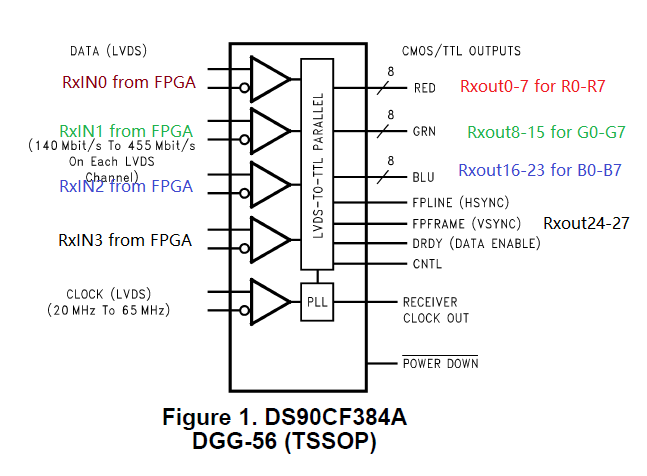
Part Number: DS90CF384A
Dear expert,
The DS90CF384A are used to convert 4 channel LVDS from FPGA to TTL. Can the pin of LVDS and TTL be mapped as follows? If not, how to map the RxIN to RxOUT?
- LVDS_0 from FPGA connected to RxIN0+ and RxIN0- pin, and TTL output by Rxout0-7 pin
- LVDS_1 from FPGA connected to RxIN1+ and RxIN01- pin, and TTL output by Rxout8-15 pin
- LVDS_2 from FPGA connected to RxIN2+ and RxIN02- pin, and TTL output by Rxout16-23 pin