This thread has been locked.

If you have a related question, please click the "Ask a related question" button in the top right corner. The newly created question will be automatically linked to this question.

SN65DP159: No MAIN LINK TMDS Outputs

Part Number: SN65DP159
Other Parts Discussed in Thread: TMDS181, DP159RGZEVM

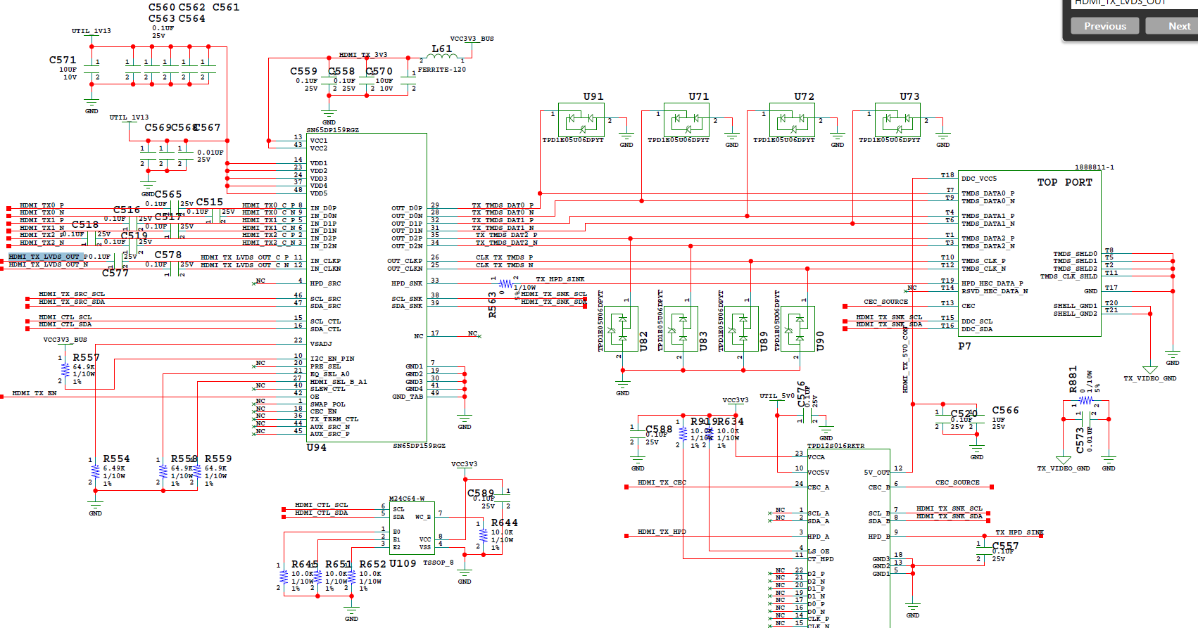
Currently on our new development board, we are not able to get any TMDS signals output from SN65DP159 to HDMI2.0 port. I2C initialization and HPD is working. 3.3V and 1.1V are good. We are output TMDS clock and data from Kintex KC7K325T to SN65DP159.

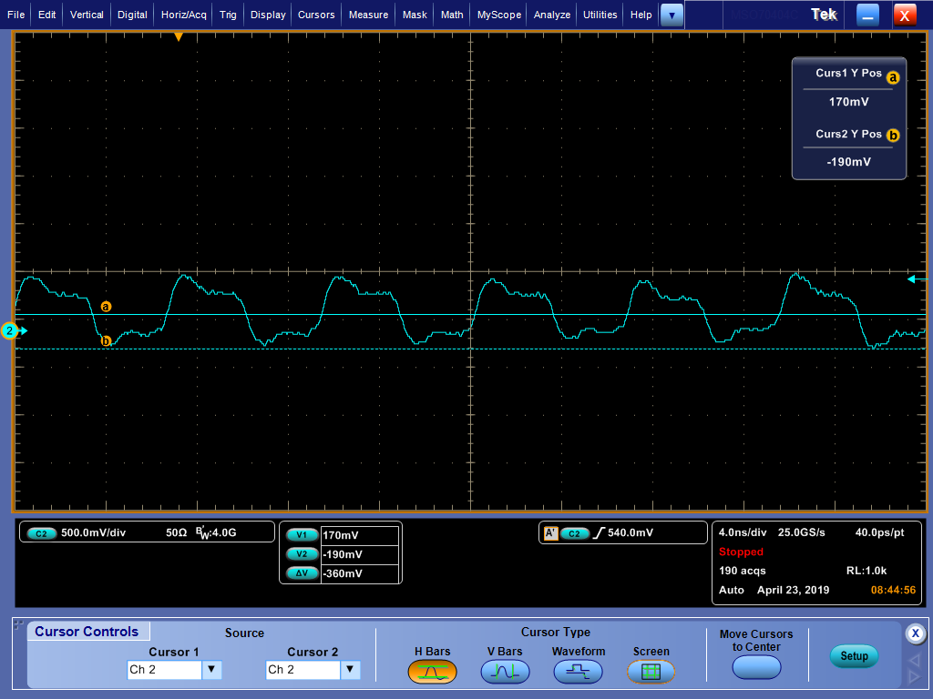
OE signal is high, HPD signal is high, 09h[3] is 0 and operate in re-driver mode. But nothing comes out from the main link outputs.

We are running out of ideas to try. Please give us some advice to trouble shoot this issue.

Thanks.

John

  • John

    Would you please your schematic?

    For TMDS clock and data, is this a AC coupled or a DC coupled output?

    Thanks
    David
  • Hi David,

    I work with John. We are using DC coupled output to the HDMI connector. Please see the attached for the schematic.

    p11.pdfctor

  • HDMI is a 3.3V common mode DC coupled output, but DP159 is a AC coupled input with common mode voltage of min 0V and max 2V. You need to provide an external termination network to correctly set the common mode voltage. But with external termination, you need to double output amplitude to account for the double termination.

    Another choice is to to use TMDS181 which is a DC coupled input, so no external AC caps or termination network is needed.

    Thanks
    David
  • Hi David,

    Thanks for your comment.

    I am confused because this chip is designed for AC coupled input, and it does have internal termination to Vbias, why we still need to provide external termination to 3.3V to make it work.

    We were following Xilinx's reference design shown below. I did not see any external termination, however their dev kit works fine. 

    Below is the measured waveform of the input clock to DP159 before the capacitor with common voltage of 1.2V

    Below is the measured waveform of the input clock to DP159 after the capacitor with common voltage of 170mV.

    Please advise, thank you.

  • Can you probe the clock output and also dump out the DP159 register, both page 0 and page 1 (write 0x01b to register 0xFFh)?

    Thanks
    David
  • Hi David,

    I have attached .txt file for the dump out.

    The out put clock is flat at around 3.3v, seems to be idle.

    We also have input data with common voltage at 1v before capacitor. The output data is flat around 0v.

    Thanks,

    Harry

    dp159_settings.txt
    dp159 page 0
    00: 44
    01: 50
    02: 31
    03: 35
    04: 39
    05: 20
    06: 20
    07: 20
    08: 01
    09: 06
    0A: 31
    0B: 80
    0C: 48
    0D: 00
    0E: 00
    0F: 0F
    10: 00
    11: 00
    12: 00
    13: 00
    14: 00
    15: 00
    16: 00
    17: F0
    18: 00
    19: 00
    1A: 00
    1B: 00
    1C: 00
    1D: 00
    1E: 15
    1F: 0B
    20: 4A
    21: 00
    22: 00
    23: 00
    24: 00
    25: 00
    26: 00
    27: 00
    28: 00
    29: 00
    2A: 00
    2B: 00
    2C: 00
    2D: 00
    2E: 00
    2F: 00
    30: 00
    31: 00
    32: 00
    33: 00
    34: 00
    35: 00
    36: 00
    37: 00
    38: 00
    39: 00
    3A: 00
    3B: 00
    3C: 00
    3D: 00
    3E: 00
    3F: 00
    40: 00
    41: 00
    42: 00
    43: 00
    44: 00
    45: 00
    46: 00
    47: 00
    48: 00
    49: 00
    4A: 00
    4B: 00
    4C: 00
    4D: 00
    4E: 00
    4F: 00
    50: 00
    51: 00
    52: 00
    53: 00
    54: 00
    55: 00
    56: 00
    57: 00
    58: 00
    59: 00
    5A: 00
    5B: 00
    5C: 00
    5D: 00
    5E: 00
    5F: 00
    60: 00
    61: 00
    62: 00
    63: 00
    64: 00
    65: 00
    66: 00
    67: 00
    68: 00
    69: 00
    6A: 00
    6B: 00
    6C: 00
    6D: 00
    6E: 00
    6F: 00
    70: 00
    71: 00
    72: 00
    73: 00
    74: 00
    75: 00
    76: 00
    77: 00
    78: 00
    79: 00
    7A: 00
    7B: 00
    7C: 00
    7D: 00
    7E: 00
    7F: 00
    80: 00
    81: 00
    82: 00
    83: 00
    84: 00
    85: 00
    86: 00
    87: 00
    88: 00
    89: 00
    8A: 00
    8B: 00
    8C: 00
    8D: 00
    8E: 00
    8F: 00
    90: 00
    91: 00
    92: 00
    93: 00
    94: 00
    95: 00
    96: 00
    97: 00
    98: 00
    99: 00
    9A: 00
    9B: 00
    9C: 00
    9D: 00
    9E: 00
    9F: 00
    A0: 00
    A1: 00
    A2: 00
    A3: 00
    A4: 00
    A5: 00
    A6: 00
    A7: 00
    A8: 00
    A9: 00
    AA: 00
    AB: 00
    AC: 00
    AD: 00
    AE: 00
    AF: 00
    B0: 00
    B1: 00
    B2: 00
    B3: 00
    B4: 00
    B5: 00
    B6: 00
    B7: 00
    B8: 00
    B9: 00
    BA: 00
    BB: 00
    BC: 00
    BD: 00
    BE: 00
    BF: 00
    C0: 00
    C1: 00
    C2: 00
    C3: 00
    C4: 00
    C5: 00
    C6: 00
    C7: 00
    C8: 00
    C9: 00
    CA: 00
    CB: 00
    CC: 00
    CD: 00
    CE: 00
    CF: 00
    D0: 00
    D1: 00
    D2: 00
    D3: 00
    D4: 00
    D5: 00
    D6: 00
    D7: 00
    D8: 00
    D9: 00
    DA: 00
    DB: 00
    DC: 00
    DD: 00
    DE: 00
    DF: 00
    E0: 00
    E1: 00
    E2: 00
    E3: 00
    E4: 00
    E5: 00
    E6: 00
    E7: 00
    E8: 00
    E9: 00
    EA: 00
    EB: 00
    EC: 00
    ED: 00
    EE: 00
    EF: 00
    F0: 00
    F1: 00
    F2: 00
    F3: 00
    F4: 00
    F5: 00
    F6: 00
    F7: 00
    F8: 00
    F9: 00
    FA: 00
    FB: 00
    FC: 00
    FD: 00
    FE: 00
    dp159 page 1
    00: 02
    01: 00
    02: 3F
    03: 00
    04: A0
    05: 00
    06: 00
    07: 00
    08: 04
    09: 00
    0A: 00
    0B: 33
    0C: 00
    0D: 00
    0E: 11
    0F: 00
    10: F0
    11: 00
    12: 20
    13: 07
    14: 00
    15: 00
    16: 00
    17: 00
    18: 00
    19: 00
    1A: 00
    1B: 00
    1C: 00
    1D: 00
    1E: 00
    1F: 00
    20: 00
    21: 00
    22: 00
    23: 00
    24: 00
    25: 00
    26: 00
    27: 00
    28: 00
    29: 00
    2A: 00
    2B: 00
    2C: 00
    2D: 00
    2E: 00
    2F: 00
    30: 70
    31: 30
    32: 0F
    33: 80
    34: 00
    35: 00
    36: 00
    37: 00
    38: 08
    39: 08
    3A: 08
    3B: 08
    3C: 04
    3D: 06
    3E: 00
    3F: 00
    40: 80
    41: 80
    42: 80
    43: 80
    44: FF
    45: 00
    46: 00
    47: 00
    48: FF
    49: FF
    4A: FF
    4B: FF
    4C: 03
    4D: 20
    4E: 77
    4F: 77
    50: 00
    51: 00
    52: 00
    53: 00
    54: 00
    55: 00
    56: 00
    57: 00
    58: 00
    59: 00
    5A: 00
    5B: 00
    5C: 40
    5D: 40
    5E: 40
    5F: 40
    60: 00
    61: 00
    62: 00
    63: 00
    64: 00
    65: 00
    66: 00
    67: 00
    68: 00
    69: 00
    6A: 00
    6B: 00
    6C: 00
    6D: 00
    6E: 00
    6F: 00
    70: 00
    71: 00
    72: 00
    73: 00
    74: 00
    75: 00
    76: 00
    77: 00
    78: 00
    79: 00
    7A: 00
    7B: 00
    7C: 00
    7D: 00
    7E: 00
    7F: 00
    80: 00
    81: 10
    82: 00
    83: 00
    84: 00
    85: 00
    86: 00
    87: 00
    88: 00
    89: 00
    8A: 00
    8B: 00
    8C: 00
    8D: 00
    8E: 00
    8F: 00
    90: 00
    91: 00
    92: 00
    93: 00
    94: 00
    95: 00
    96: 00
    97: 00
    98: 00
    99: 00
    9A: 00
    9B: 00
    9C: 00
    9D: 00
    9E: 00
    9F: 00
    A0: 00
    A1: 00
    A2: 0A
    A3: 00
    A4: 00
    A5: 00
    A6: 00
    A7: 00
    A8: 00
    A9: 00
    AA: 00
    AB: 00
    AC: 00
    AD: 00
    AE: 00
    AF: 00
    B0: F4
    B1: 02
    B2: 00
    B3: 00
    B4: 00
    B5: 00
    B6: 00
    B7: 00
    B8: 00
    B9: 00
    BA: 00
    BB: 00
    BC: 00
    BD: 00
    BE: 00
    BF: 00
    C0: 00
    C1: 00
    C2: 00
    C3: 00
    C4: 00
    C5: 00
    C6: 00
    C7: 00
    C8: 00
    C9: 00
    CA: 00
    CB: 00
    CC: 00
    CD: 00
    CE: 00
    CF: 00
    D0: 00
    D1: 00
    D2: 00
    D3: 00
    D4: 00
    D5: 00
    D6: 00
    D7: 00
    D8: 00
    D9: 00
    DA: 00
    DB: 00
    DC: 00
    DD: 00
    DE: 00
    DF: 00
    E0: 00
    E1: 00
    E2: 00
    E3: 00
    E4: 00
    E5: 00
    E6: 00
    E7: 00
    E8: 00
    E9: 00
    EA: 00
    EB: 00
    EC: 00
    ED: 00
    EE: 00
    EF: 00
    F0: 00
    F1: 00
    F2: 00
    F3: 00
    F4: 00
    F5: 00
    F6: 00
    F7: 00
    F8: 00
    F9: 00
    FA: 00
    FB: 00
    FC: 00
    FD: 00
    FE: 00

  • Harry

    Can you please check the voltage on HPD_SRC and HPD_SNK?

    Also, can you capture the power up ramp timing between VCC, VDD, and OE?

    Last. can you write to page 0 register 0x0Bh, bit [4:3] and change the termination to 75-150ohm (0x11b)?

    On the clock output measurement, how do you do it? Do you just probe the clock when there is a sink attached or have a scope connected directly to the clk output? If the scope is connected directly to clk output, do you have HPD_SNK high and also have 50ohm pull up to 3.3V on the clock?

    Thanks
    David
  • Hi David,

    At first, we have HPD 2.8v at the HDMI TX receptacle pin. After a voltage divider, HPD_SNK is 1.6v.

    From the datasheet, HPD_SNK of 1.6v (< 2.1v) will be considered low. But the HPD_SRC is 2.8v...

    Then we removed the voltage divider resistor R28.

    Now we have HPD_SNK at 2.8v, HPD_SRC is also 2.8v.

    Still no output.

    We also tried to set the register per your advice, but got the same result.

    Yet we only probed when the sink was attached, with HPD_SNK high, but without 50 ohm pull up to 3.3v.

    I will try to catch the power ramp and update you.

    Meanwhile, please advise if you have any thought.

    Thank you very much.

  • Harry

    Any chance you can ship the board to me so I can look at it in the lab?

    Thanks
    David
  • Hi David,

    Thanks for providing the opportunity for the lab test.

    We had some progress this morning, maybe we do not have to cost you more time in the lab.

    We made a change to the DEV_FUNC_MODE bits,

    from the default "Automatic redriver to retimer crossover at 1.0 Gbps"

    to the "Redriver mode across full range 250 Mbps to 6-Gbps".

    Then we can see our test pattern in the monitor.

    Until now, we are able to see up to  8 bits YUV444 @ 4K30FPS.

    However it seems the retimer mode does not work for our system.

    From DP159 datasheet, I can see the input clock jitter tolerance is 0.3Tbit, does it mean 0.33 ps or 3.33 ps.

    We are using Si5338 clock generator as the clock source. It has 1 ps jitter. We see reference designs use Si5324, which only has 0.29 ps jitter.

    We think maybe because of the 1 ps jitter, the PLL can not be locked when configured to the retimer mode.

    Please advise, thanks.

    Harry

  • Harry

    Tbit is defined as one UI.

    The register dump provided earlier shows the PLL_LOCK_COMPLETE not being set. The PLL_LOCK_COMPLETE bit needs to be set to indicate the PLL has been locked. If it is not locked, then the retimer will not work properly.

    Thanks
    David
  • Hi David,

    Thanks for your help. 

    So far we are able to drive the HDMI display using the re-driver mode.

    But in the re-timer mode, PLL_LOCK_COMPLETE bit is not set. Can you advise what may be the cause that the PLL is not locked or how to proceed to debug the issue? We are in the process of setting up to run the EyeScan Tool. Perhaps that may help provide some insights to the signal quality at the receiver. We have also getting the EVALUATION MODULE DP159RGZEVM using as a reference. 

    Regards,

    John

  • John

    For HDMI1.4 3G, the clock frequency looks to be correct.

    Have you checked both CLK_P and CLK_N? There also appears to be pre-emphasis on the clock signal.

    Thanks
    David
  • John, Harry

    Any update to this thread?

    Thanks
    David
  • Hi David,

    Thanks for your help. After further checking, we suspect the PLL lock issue may be related to the clocking source jitter performance. We may have to re-spin the PCB and check this issue again. For the time being, re-driver mode is sufficient for our application.

    Regards,

    John