This thread has been locked.

If you have a related question, please click the "Ask a related question" button in the top right corner. The newly created question will be automatically linked to this question.

TMDS181: Unable to read sink side device EDID

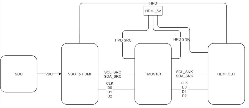
Part Number: TMDS181

Hi teams

My customer is using TMDS181 in their new design and an issue has reported.

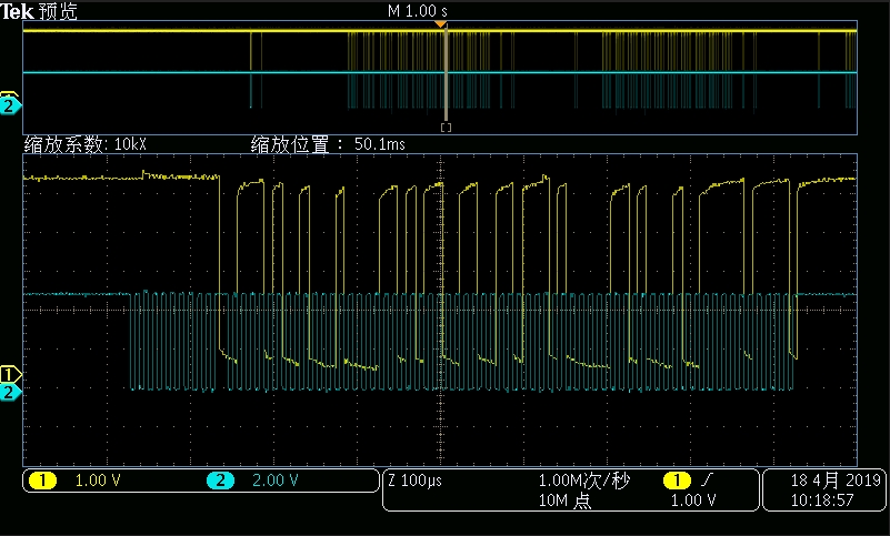
They use TMDS181 for HDMI out re-timer and found that the SCL_SNK is almost the same with SDA_SNK.

The waveform is shown below:

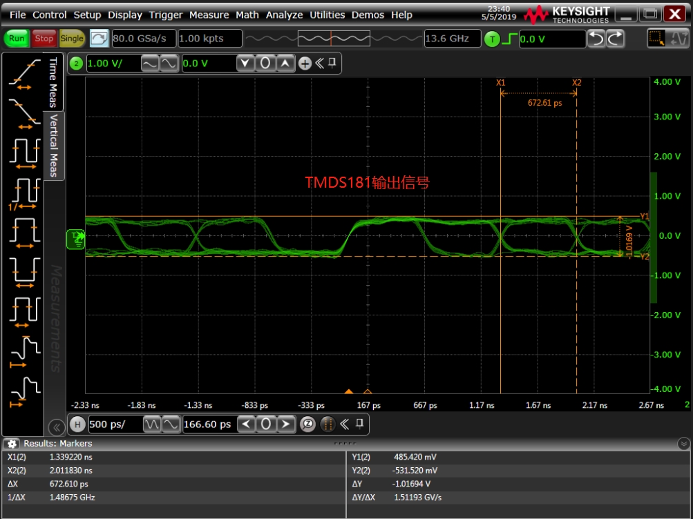
The second picture is SCL_CRC and SDA_SRC waveform.

  • Gabriel

    Please use the TMDS181 snoop configuration where the SDA/SCL from the source is connected directly to the SDA/SCL of the sink. The TMDS181 will need its SDA_SNK and SCL_SNK pins connected to this link in order to correctly configure the TMDS_CLOCK_RATIO_STATUS bit. This is shown in Figure 35 of the datasheet.

    Thanks
    David
  • Hi David

    I have another question about TMDS181 need your help to figure it out.

    I found below reference schematic in datasheet. PIN 1/10/17/20/21/27/36 is connected to both pull up and pull down resistor.

    I found some of them(such as PIN20/PIN21) is 3 level pin. These pin is make sense to me to do so.

    But i wondering to know why we need to connect 2 resistor in the same time for non 3 level pin?

  • Gabriel

    The reference schematic shows the possible connection for these pins. You can tie them either high, low, or NC. It does not mean you have to tie them to both pullup and pulldown at the same time.

    Thanks
    David
  • Hi David

    Another issue reported from the customer.

    Cutomer used it in TV as HDMI out re-timer so it should be source side application.

    Customer configure it in I2C mode and use default setting. 

    The video source output 4K@60HZ signal to TMDS181 so it should be a signal up to 5.6Ghz.

    But they probe the output signal and found that it only have 1.5Ghz. And they have already probe the input signal and confirmed that the input signal is 5.6Ghz.

    Below is the wavefrom captured by customer.

    Are any configuration need to be done in 4K operation?

  • Gabriel

    Please have TX_TERM_CTL set to 0x11b (75ohm to 150ohm). Can they dump out the entire TMDS181 register, both page 0 and page 1(write 0x01b to address 0xFFh first)?

    Thanks
    David
  • Hi David
    You mean that write 0x01b to address 0xFFh could dump out the entire TMDS181 register?
    I didn't find this feature in the datasheet.
  • Gabriel

    The datasheet only includes page 0 register which the customer can dump out directly.

    In addition to the page 0 register, there are Page 1 hidden registers. To dump out these hidden registers, please write 0x01b to 0xFFh register first and then dump out the registers.

    Thanks
    David
  • Hi David
    For TX_Term_CTL setting do you mean we need to connect a 75ohm~150ohm resistor between this pin and ground?
  • Gabriel

    Since TMDS181 is in I2C control mode, the TX_TERM_CTL bit, not the pin must be set manually depending on the source. When the source is HDMI1.4, the TX_TERM_CTL bit must be set to 150-300ohm. When the source is HDMI2.0, the TX_TERM_CTL bit must be set to 75 to 150ohm.

    Thanks
    David
  • Hi David

    The DDC issue has been fixed. It caused by another device.

    I want to update the latest issue background.

    Customer requirement:

    1. They don't want to do DDC communication.
    2. They want to output always output HDMI2.0 high-speed signal no matter what device plugin.

    As they don't want to do register initialization configuration again when a sink device plugin or plug out. So they plug both SNK/SRC HPD to HDMI5V.

    1. When the system is powered up without a monitor connection. The TMDS_CLOCK_RATIO_STATUS read back 1.
    2. When the system is powered up with a monitor connection. The TMDS_CLOCK_RATIO_STATUS read back 0.

    No matter with or without the monitor, customer system SOC won't output HDMI signal after TMDS181 power up. Until SOC receive a commend from user it will start output HDMI signal but TMDS181 didn't have output signal. Customer needs to disable SOC HDMI output and enable it again and repeat 3-4 time the TMDS181 will have possibility output normally.

    Below is my question:

    1. In TMDS_CLOCK_RATIO_STATUS register description it said :
      When bit 1 of address 0xA8 offset 0x20 in the SCDC register set is written
      to a 1’b1, then this field will be set to a 1’b1. When bit 1 of address 0xA8 offset 0x20
      is written to a 1’b0, then this field will be set to a 1’b0.
      I want to know if i want to keep this bit always set to 1 should i disable DDC_training function?
    2. Which the register bit it means "0x20"?  TMDS181 0x20  have two bit.
    3. Are this issue is relative with signal detect function? 
    4. In datasheet 9.2.1.1 it said OE pin need to change states after the power railed stabilized. What dose it mean? Customer connect OE with GND through a 104 cap without GPIO control.

  • Gabriel

    Is this a close or open design? Are they only going to have HDMI2.0 display connected to their system?

    Part of the DDC communication is to enable the display to communicate its supported display modes to the SOC. But a HDMI1.4 display will not work at HDMI2.0.

    Thanks
    David
  • Hi David
    It's a close design.
    So want it outputs HDMI2.0 signal all the time. Could you help to give some comments on my previous questions?
  • Gabriel

    Assume the SOC is sending out the proper HDMI2.0 signal and clock, for TMDS181:

    You need to disable DDC training
    Set TMDS_CLK_RATIO bits to 1/40
    Set TX_TERM_CTL bits to 75 to 150ohm

    Slave address 0xA8 offset 0x20 is the SCDC register, not the TMDS181 register.

    Please refer to section 8.3.1 for OE implementation, have a pulldown capacitor is ok as long as they meet the power-up timing requirement as shown in Figure 1 and Table 6.9.

    Thanks
    David
  • Gabriel

    Do you have an update?

    Thanks

    David

  • Hi David

    Thanks for your support.

    The original issue has been fixed by disabling DDC training function.

    Customer has several new questions want to figure out:

    1. Do you mean that 0xA8 offset 0x20 is the sink device register? Or SCDC register is sink device register?
    2. How DDC training work to change CLOCK Ratio bit?
    3. Customer also used this device in SINK application but they didn't follow our reference design to connect SOC DDC to the connector directly. They connect the DDC interface through the TMDS181. They want to know what the major different between two configuration? Why TI recommend the first one?
    4. Are the HPD pin control logic is different in SINK mode and SOURCE mode?

  • Gabriel

    1. Please refer to HDMI Spec 2.0b, section 6.1.3.2 for the information on TMDS_CLOCK_RATIO_STATUS bit. When a sink supports data rate above 3.4G, the sink needs to provide a write/read TMDS_CLOCK_RATIO_STATUS control bit. When configure the TMDS link for operation below 3.4G, the source write a "0" to the TMDS_CLOCK_RATIO_STATUS bit. When configure the TMDS link for operation between 3.4G and 6G, the source writes a "1" to the TMDS_CLOCK_RATIO_STATUS bit. The TMDS181 will snoop this write as part of the DDC training and set its own TMDS_CLOCK_RATIO_STATUS bit accordingly.

    2. When DDC training is disabled, then the TMDS181 will not snoop and the TMDS_CLOCK_RATIO_STATUS bit must be set manually.

    3. Please see section 8.4.4 and particularly the NOTE section.

    4. There is no SINK mode or SOURCE mode for TMDS181. For sink, HPD is an output and for source HPD is an input.

    Thanks
    David