This thread has been locked.

If you have a related question, please click the "Ask a related question" button in the top right corner. The newly created question will be automatically linked to this question.

SN65DSI86: driver code

Part Number: SN65DSI86
Other Parts Discussed in Thread: TEST2

Hello Team,

SN65DSI86 is used as the transceiver from MIPI DSI to eDP.

The user is implementing driver code based on the linked source.

 https://github.com/torvalds/linux/blob/master/drivers/gpu/drm/bridge/ti-sn65dsi86.c

I2C access is okay, but it cannot get the information from panel.

Please help to solve the following issue.

We are trying to register ti-sn65dsi86 (mipi DSI to eDP bridge) driver in i.MX8QXP.


As far as I understand, following shall be the link of the nodes in the DTSI:

MIPI_DSI1 -> MIPI_DSI_BRIDGE1 -> eDP_BRIDGE > PANEL

To do so we  have added the driver and done modifications in the DTSI (please find attached file). Please note that the customer uses the eDP bridge on i2c0_csi0 pad group and not the default i2c0_mipi_lvds0 for MIPI DSI display configuration and pinctrl changes were similarly done.


We are able to probe the I2C slave device (edp bridge) at 0x2c, but it fails to find a DRM Panel. We are trying to display on HDMI monitor of 1920x1080 resolution and used a panel (from panel-simple.c) similar to this.


We also have a query on how to register the drm_dp_aux_register for eDP bridge. We have added the i2c-bus node in the edp-bridge in dtsi to register the sub device of i2c. Is this the correct way to do it?


Please find the related logs as below:


root@imx8qxpdsw:~# dmesg  | grep -i drm
[    0.000000] Kernel command line: console=ttyLP0,115200 earlycon=lpuart32,0x5a060000,115200 root=/dev/mmcblk0p2 rootwait rw quiet drm.debug=0x3F
[    0.457928] [drm:drm_core_init] Initialized
[    0.463890] [drm:ti_sn_bridge_probe] *MSS* 685:: Enter Probe of DSI86
[    0.470541] [drm:ti_sn_bridge_probe] *MSS* 691::
[    0.475440] [drm:ti_sn_bridge_probe] *MSS* 698::
[    0.480339] drm_of_find_panel_or_bridge:262:: node edp-bridge
[    0.486267] drm_of_find_panel_or_bridge:263:: node /i2c@58226000/edp-bridge@2c
[    0.511456] [drm:ti_sn_bridge_probe] *ERROR* could not find any panel node
[    0.518346] [drm:ti_sn_bridge_probe] *MSS* 706:: node edp-bridge
[    0.524541] [drm:ti_sn_bridge_probe] refclk not found
[    0.524548] [drm:ti_sn_bridge_probe] *MSS* 720::
[    0.529503] [drm:ti_sn_bridge_probe] *MSS* 728::
[    0.534407] [drm:ti_sn_bridge_probe] *ERROR* failed to get enable gpio from DT
[    0.541641] [drm:ti_sn_bridge_probe] *MSS* 740::
[    0.546705] [drm:ti_sn_bridge_probe] *MSS* 747::
[    0.564441] [drm:ti_sn_bridge_probe] *MSS* 758::
[    0.569486] [drm:drm_dp_aux_register_devnode] drm_dp_aux_dev: aux [ti-sn65dsi86-aux] registered as minor 0
[    0.569644] [drm:ti_sn_bridge_probe] *MSS* 772::
[    0.574537] [drm:ti_sn_bridge_probe] *MSS* 775::


root@imx8qxpdsw:~# i2cdetect -l

i2c-3   i2c             ti-sn65dsi86-aux                        I2C adapter

i2c-1   i2c             56246000.i2c                            I2C adapter

i2c-2   i2c             5a810000.i2c                            I2C adapter

i2c-0   i2c             58226000.i2c                            I2C adapter

root@imx8qxpdsw:~# i2cdetect 0

WARNING! This program can confuse your I2C bus, cause data loss and worse!

I will probe file /dev/i2c-0.

I will probe address range 0x03-0x77.

Continue? [Y/n] y

     0  1  2  3  4  5  6  7  8  9  a  b  c  d  e  f

00:          -- -- -- -- -- -- -- -- -- -- -- -- --

10: -- -- -- -- -- -- -- -- -- -- -- -- -- -- -- --

20: -- -- -- -- -- -- -- -- -- -- -- -- UU -- -- --

30: -- -- -- -- -- -- -- -- -- -- -- -- -- -- -- --

40: -- -- -- -- -- -- -- -- -- -- -- -- -- -- -- --

50: -- -- -- -- -- -- -- -- -- -- -- -- -- -- -- --

60: -- -- -- -- -- -- -- -- -- -- -- -- -- -- -- --

70: -- -- -- -- -- -- -- --


Please help us know if I'm missing some crucial settings.

  • Lloyd

    There is no driver code for DSI86, but DSI86 register do need to be programmed properly first. I sent you a spreadsheet and the customer can use it to input the panel EDID info, and then generate the DSI86 programming value.

    Thanks

    David 

  • Hi  David,

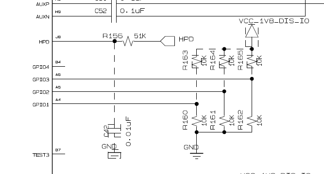
    GPIO[3:1] is 000 in the HW aspect.

    REFCLK is connected with GND.

    Also test2 pin is connected to GND.

    Here is our register dump detail.

    0 1 2 3 4 5 6 7 8 9 a b c d e f 0123456789abcdef
    00: 36 38 49 53 44 20 20 20 02 00 83 00 00 01 00 00 68ISD ?.?..?..
    10: 20 00 4c 4c 00 00 00 00 00 00 00 00 00 00 00 00 .LL............
    20: 80 07 00 00 38 04 00 00 00 00 00 00 2c 00 00 00 ??..8?......,...
    30: 05 00 00 00 94 00 24 00 58 00 04 00 00 00 00 00 ?...?.$.X.?.....
    40: 57 1e 00 00 80 00 98 08 65 04 c0 00 29 00 2c 00 W?..?.??e??.).,.
    50: 05 00 80 07 38 04 20 00 40 e4 0d 00 11 00 80 00 ?.??8? .@??.?.?.
    60: a0 60 a4 00 00 00 00 00 00 00 00 00 00 00 00 00 ?`?.............
    70: 00 00 00 00 00 01 02 00 80 00 00 00 00 00 00 00 .....??.?.......
    80: 00 00 00 00 00 00 00 00 00 1f 7c f0 c1 07 1f 7c .........?|????|
    90: f0 c1 07 10 e0 00 00 04 01 00 00 00 00 00 00 00 ?????..??.......
    a0: 01 ff ff 00 00 00 00 00 00 00 00 00 00 00 00 00 ?...............
    b0: 04 78 ac ac 08 6c 9c 9c 0c 5c 5c 5c 0c 0c 0c 0c ?x???l???\\\????
    c0: 3f 3f 0f 00 00 00 00 00 00 00 00 00 00 00 00 00 ???.............
    d0: 00 00 00 00 00 00 00 00 00 00 00 00 00 00 00 00 ................
    e0: 00 00 00 00 00 00 00 00 00 00 00 00 00 00 00 00 ................
    f0: 00 03 00 00 08 20 00 00 02 00 00 00 00 00 00 00 .?..? ..?.......

    We are trying to display on HDMI monitor using HDMI to eDP converter.

    Can you please review the register detail and let us know the issue?

    We also have tried to display using test colorbar pattern but result remains the same.

    Thanks

    Saurabh

  • Saurabh

    Would you please provide monitor's EDID information? Also, for eDP to HDMI, are you using an active eDP to HDMI converter?

    Thanks
    David
  • Hello David,

    Please find the following EDID information you asked Saurabh for:

    Section "Monitor"
    Identifier "BenQ GW2270"
    ModelName "BenQ GW2270"
    VendorName "BNQ"
    # Monitor Manufactured week 29 of 2016
    # EDID version 1.4
    # Analog Display
    Option "SyncOnGreen" "true"
    DisplaySize 480 270
    Gamma 2.20
    Option "DPMS" "true"
    Horizsync 30-83
    VertRefresh 50-76
    # Maximum pixel clock is 170MHz
    #Not giving standard mode: 1920x1080, 60Hz
    #Not giving standard mode: 1280x720, 60Hz
    #Not giving standard mode: 1280x800, 60Hz
    #Not giving standard mode: 1280x1024, 60Hz
    #Not giving standard mode: 1600x900, 60Hz
    #Not giving standard mode: 1680x1050, 60Hz
    Modeline "Mode 0" 148.50 1920 2008 2052 2200 1080 1084 1089 1125 +hsync +vsync
    EndSection

    00ff ffff ffff ff00 09d1 db78 4554 0000
    1d1a 0104 0e30 1b78 2e34 55a7 5552 a027
    1150 54a5 6b80 d1c0 81c0 8100 8180 a9c0
    b300 0101 0101 023a 8018 7138 2d40 582c
    4500 dc0c 1100 001e 0000 00ff 004d 3747
    3038 3935 3453 4c30 0a20 0000 00fd 0032
    4c1e 5311 000a 2020 2020 2020 0000 00fc
    0042 656e 5120 4757 3232 3730 0a20 003b


    Also, Yes we are using an eDP to HDMI converter to connect it to the GW2270 Benq HDMI monitor.

    Regards,
    Rizu
  • Rizu

    Attached is a color bar example script. The script assume the monitor supports 2 lane HBR. If not, please change the DSI86 register accordingly.  Please also make sure TEST2 pin is pulled high.

    Please make sure you are using an active eDP to HDMI converter, passive converter will not work.

    <aardvark> 
    <configure i2c=1 spi=1 gpio=0 tpower=1 pullups=0/> 
    <i2c_bitrate khz=100/> 
    
    ======ASSR RW control  ====== 
    <i2c_write addr=0x2D count=1 radix=16> FF 7 </i2c_write>/> 
    <i2c_write addr=0x2D count=1 radix=16> 16 1 </i2c_write>/> 
    <i2c_write addr=0x2D count=1 radix=16> FF 0 </i2c_write>/> 
    
    ======REFCLK Frequency  ====== 
    <i2c_write addr=0x2D count=1 radix=16> 0A 2 </i2c_write>/> 
    
    ======DSI Mode  ====== 
    <i2c_write addr=0x2D count=1 radix=16> 10 20 </i2c_write>/> 
    
    ======DSIA Clock  ====== 
    <i2c_write addr=0x2D count=1 radix=16> 12 21 </i2c_write>/> 
    
    ======DSIB Clock  ====== 
    <i2c_write addr=0x2D count=1 radix=16> 13 21 </i2c_write>/> 
    
    ======DP Datarate  ====== 
    <i2c_write addr=0x2D count=1 radix=16> 94 80 </i2c_write>/> 
    
    ======Enable PLL  ====== 
    <i2c_write addr=0x2D count=1 radix=16> 0D 1 </i2c_write> <sleep ms=10/> 
    
    ======Enable enhanced frame  in DSI86  ====== 
    <i2c_write addr=0x2D count=1 radix=16> 5A 4 </i2c_write>/> 
    
    ======Number of DP lanes  ====== 
    <i2c_write addr=0x2D count=1 radix=16> 93 20 </i2c_write>/> 
    
    ======Start Semi-Auto Link Training  ====== 
    <i2c_write addr=0x2D count=1 radix=16> 96 0A </i2c_write> <sleep ms=20/> 
    
    ======CHA Active Line Length  ====== 
    <i2c_write addr=0x2D count=2 radix=16> 20 80 07 </i2c_write>/> 
    
    ======CHB Active Line Length  ====== 
    <i2c_write addr=0x2D count=2 radix=16> 22 0 0 </i2c_write>/> 
    
    ======Vertical Active Size   ====== 
    <i2c_write addr=0x2D count=2 radix=16> 24 38 04 </i2c_write>/> 
    
    ======Horizontal Pulse Width   ====== 
    <i2c_write addr=0x2D count=2 radix=16> 2C 2C 00 </i2c_write>/> 
    
    ======Vertical Pulse Width   ====== 
    <i2c_write addr=0x2D count=2 radix=16> 30 05 00 </i2c_write>/> 
    
    ======HBP   ====== 
    <i2c_write addr=0x2D count=1 radix=16> 34 94 </i2c_write>/> 
    
    ======VBP   ====== 
    <i2c_write addr=0x2D count=1 radix=16> 36 24 </i2c_write>/> 
    
    ===== HFP  ====== 
    <i2c_write addr=0x2D count=1 radix=16> 38 58 </i2c_write>/> 
    
    ===== VFP  ====== 
    <i2c_write addr=0x2D count=1 radix=16> 3A 04 </i2c_write>/> 
    
    ===== DP-18BPP Disable  ====== 
    <i2c_write addr=0x2D count=1 radix=16> 5B 0 </i2c_write>/> 
    
    ===== Color Bar Enable  ====== 
    <i2c_write addr=0x2D count=1 radix=16> 3C 17 </i2c_write>/> 
    
    ===== Enhanced Frame, and Vstream Enable  ====== 
    <i2c_write addr=0x2D count=1 radix=16> 5A 0C </i2c_write>/> 
    
    </aardvark> 


    Thanks

    David

  • Hello David,

    Thanks for your suggestions. We used the example script for our reference, with modifications as per our use case, but were not successful to get the display working.

    In our hardware, the TEST2 pin is grounded. It may be a probable reason as to why the display is not functional for a color bar test pattern.

    Is there any other software configuration possible to workaround this?  At this stage, HW modification is not possible so we need to verify this with TEST2 pin connected to GND.

    Regards,

    Rizu

  • Hello David,

    We are also facing an issue to read the EDID info of the connected panel.

    Please note that the reference driver at github.com/.../ti-sn65dsi86.c didn't have this, we have added the code to fetch the EDID in ti_sn_bridge_connector_get_modes() function.

    The datasheet, on page 20: step 9, says that:

    Resolution capability of eDP Panel through reading EDID. In a eDP application, the Panel resolution capability may be known
    in advance.

    The methods suggested further that this can be done through aux requests using I2C-Over-Aux registers. Currently, we are facing an issue to read these registers.

    May you suggest a way as to how can the EDID info be added? Does it require communication with the panel over I2C or can there be a workaround?

    Regards,

    Rizu

  • Rizu

    EDID information is obtained by I2C over AUX transactions. You can do it either using the direct method or the indirect method. Below is the script example of reading EDID using the direct method.

    Read Sink’s EDID (Direct Method)
    This script will read 256 bytes of the EDID.
    <aardvark>
    <configure i2c="1" spi="1" gpio="0" tpower="1" pullups="0" />
    <i2c_bitrate khz="100" />
    ======Enable I2C_ADDR_CLAIM1======
    <i2c_write addr="0x2D" count="1" radix="16">60 A1</i2c_write> />
    ======Write EDID base of 00 ======
    <i2c_write addr="0x50" count="0" radix="16">00</i2c_write> />
    ======Read 256 bytes of EEID======
    <i2c_read addr="0x50" count="256" radix="16">00</i2c_read> />
    </aardvark>

    TEST2 pin must be pulled high in order to disable ASSR.

    Thanks
    David
  • Hi David,

    Much thanks for your assistance!

    We have done the HW modification to pull high the Test2 pin.

    • Previously the 0x5A register read 0x0d ( ASSR_CONTROL bits = 01 for ASSR ).
    • After the HW modification and SW config to disable ASSR, it now reads 0x0C ( ASSR_CONTROL bits = 00 for Standard )

    However, we are still not able to get the display up. We have tried to use a DP monitor instead of HDMI. Please find the attached file with the EDID info for the same.

    We have some queries further:

    • What is the significance of the I2C-over-Aux registers? We are not able to probe/read any of the registers there. Please check the following logs. Note that the edp bridge is on i2c-0.

    root@imx8qxpdsw:~# i2cdetect -l

    i2c-3   i2c         ti-sn65dsi86-aux         I2C adapter

    i2c-1   i2c         56246000.i2c              I2C adapter

    i2c-2   i2c         5a810000.i2c            I2C adapter

    i2c-0   i2c         58226000.i2c              I2C adapter

    root@imx8qxpdsw:~# i2cdetect 3

    WARNING! This program can confuse your I2C bus, cause data loss and worse!

    I will probe file /dev/i2c-3.

    I will probe address range 0x03-0x77.

    Continue? [Y/n] y

         0 1 2 3 4 5 6 7 8 9 a b c d e f

    00:         -- -- -- -- -- -- -- -- -- -- -- -- --

    10: -- -- -- -- -- -- -- -- -- -- -- -- -- -- -- --

    20: -- -- -- -- -- -- -- -- -- -- -- -- -- -- -- --

    30: -- -- -- -- -- -- -- -- -- -- -- -- -- -- -- --

    40: -- -- -- -- -- -- -- -- -- -- -- -- -- -- -- --

    50: -- -- -- -- -- -- -- -- -- -- -- -- -- -- -- --

    60: -- -- -- -- -- -- -- -- -- -- -- -- -- -- -- --

    70: -- -- -- -- -- -- -- --

    Is the above behavior conventional? If not, do you have some ideas where we should check to rectify this? Is there any software configuration we are missing?

    • So currently, we are not able to get the EDID data because the I2C-Over-Aux transactions fail. How will this affect the display? Even if the EDID cannot be fetched, some display should have been obtained even at the cost of some mismatch in the resolution configuration.

    Can you please tell me if my understanding is right?

    • Can the DP monitor, with ASSR disabled function well? A piece of information from the datasheet seems a little confusing:

    In Section 8.4.2, Step 13, It states that: The SN65DSI86 only supports ASSR Display Authentication method and this method is enabled by default. An eDP panel must support this Authentication method

    So, how do we configure the DP monitor to get the display functional? Does that need to support ASSR and we need to enable it back? If yes, for what use case does the ASSR is disabled?

    • Is it possible that due to no I2C-Over-Aux transactions, some essential feature of the driver does not get enabled and due to that the display is not functional?


    Regards, 

    Rizu

    Monitor Asset Manager Report, generated 2019-05-15
    Copyright (c) 1995-2019, EnTech Taiwan.
    ---------------------------
    
    Monitor #1 [Real-time 0x1900]
      Model name............... DELL P2417H
      Manufacturer............. Dell
      Plug and Play ID......... DELA0DB
      Serial number............ R8P39817929B-959592770
      Manufacture date......... 2018, ISO week 2
      Filter driver............ None
      -------------------------
      EDID revision............ 1.4
      Input signal type........ Digital (DisplayPort)
      Color bit depth.......... 8 bits per primary color
      Color encoding formats... RGB 4:4:4, YCrCb 4:4:4, YCrCb 4:2:2
      Screen size.............. 530 x 300 mm (24.0 in)
      Power management......... Active off/sleep
      Extension blocs.......... None
      -------------------------
      DDC/CI................... Supported
      MCCS revison............. 2.1
      Display technology....... TFT
      Controller............... Mstar 0x56
      Firmware revision........ 1.2
      Firmware flags........... 0x006245CC
      Active power on time..... 1359 hours
      Power consumption........ Not supported
      Current frequency........ 67.20kHz, 59.70Hz
    
    Color characteristics
      Default color space...... Non-sRGB
      Display gamma............ 2.20
      Red chromaticity......... Rx 0.652 - Ry 0.336
      Green chromaticity....... Gx 0.321 - Gy 0.610
      Blue chromaticity........ Bx 0.153 - By 0.061
      White point (default).... Wx 0.313 - Wy 0.329
      Additional descriptors... None
    
    Timing characteristics
      Horizontal scan range.... 30-83kHz
      Vertical scan range...... 56-76Hz
      Video bandwidth.......... 170MHz
      CVT standard............. Not supported
      GTF standard............. Not supported
      Additional descriptors... None
      Preferred timing......... Yes
      Native/preferred timing.. 1920x1080p at 60Hz (16:9)
        Modeline............... "1920x1080" 148.500 1920 2008 2052 2200 1080 1084 1089 1125 +hsync +vsync
    
    Standard timings supported
         720 x  400p at  70Hz - IBM VGA
         640 x  480p at  60Hz - IBM VGA
         640 x  480p at  75Hz - VESA
         800 x  600p at  60Hz - VESA
         800 x  600p at  75Hz - VESA
        1024 x  768p at  60Hz - VESA
        1024 x  768p at  75Hz - VESA
        1280 x 1024p at  75Hz - VESA
        1152 x  864p at  75Hz - VESA STD
        1280 x 1024p at  60Hz - VESA STD
        1600 x  900p at  60Hz - VESA STD
        1920 x 1080p at  60Hz - VESA STD
    
    Report information
      Date generated........... 2019-05-15
      Software revision........ 2.91.0.1043
      Data source.............. Real-time 0x1900
      Operating system......... 10.0.15063.2
    
    Raw data
      00,FF,FF,FF,FF,FF,FF,00,10,AC,DB,A0,42,39,32,39,02,1C,01,04,A5,35,1E,78,3A,05,65,A7,56,52,9C,27,
      0F,50,54,A5,4B,00,71,4F,81,80,A9,C0,D1,C0,01,01,01,01,01,01,01,01,02,3A,80,18,71,38,2D,40,58,2C,
      45,00,0F,28,21,00,00,1E,00,00,00,FF,00,52,38,50,33,39,38,31,37,39,32,39,42,0A,00,00,00,FC,00,44,
      45,4C,4C,20,50,32,34,31,37,48,0A,20,00,00,00,FD,00,38,4C,1E,53,11,01,0A,20,20,20,20,20,20,00,A1
    
    ---------------------------
    
    Hardware data
      BUS_SLOT = PCI00000.PCI00004.PCI00008.PCI0000C.PCI00010.PCI00014.PCI00018.PCI0001C
      00000000 = 59048086.20900006.06000002.00000000.00000000.00000000.00000000.00000000
      00000010 = 59168086.00100407.03000002.00000000.EB000004.00000000.A000000C.00000000
      00000020 = 19038086.00900006.11800002.00000000.FE020004.00000000.00000000.00000000
      000000A0 = 9D2F8086.02900406.0C033021.00800000.EC230004.00000000.00000000.00000000
      000000A2 = 9D318086.00100002.11800021.00000000.EC259004.00000000.00000000.00000000
      000000A8 = 9D608086.00100400.11800021.00800000.FE03C004.00000000.00000000.00000000
      000000A9 = 9D618086.00100400.11800021.00800000.FE035004.00000000.00000000.00000000
      000000AA = 9D628086.00100400.11800021.00800000.FE034004.00000000.00000000.00000000
      000000B0 = 9D3A8086.00100406.07800021.00800000.FE02F004.00000000.00000000.00000000
      000000B8 = 282A8086.02B00407.01040021.00000000.EC250000.EC254000.0000F091.0000F081
      000000E0 = 9D108086.00100406.060400F1.00810000.00000000.00000000.00010100.200000F0
      000000E2 = 9D128086.00100406.060400F1.00810000.00000000.00000000.00020200.200000F0
      000000E4 = 9D148086.00100406.060400F1.00810000.00000000.00000000.003B0300.200000F0
      000000F8 = 9D4E8086.00000403.06010021.00800000.00000000.00000000.00000000.00000000
      000000FA = 9D218086.00000000.05800021.00800000.EC24C000.00000000.00000000.00000000
      000000FB = 9D718086.00100006.04030021.00002000.FE030004.00000000.00000000.00000000
      000000FC = 9D238086.02800003.0C050021.00000000.EC252004.00000000.00000000.00000000
      000000FE = 15D78086.00100406.02000021.00000000.EC200000.00000000.00000000.00000000
      00000100 = 525A10EC.00100406.FF000001.00000000.00000000.EC1FF000.00000000.00000000
      00000200 = 24FD8086.00100406.02800078.00000000.EC0FE004.00000000.00000000.00000000
      00000300 = 15DA8086.00100406.06040002.00010020.00000000.00000000.003B0403.000001F1
      00000400 = 15DA8086.00100406.06040002.00010020.00000000.00000000.00050504.000001F1
      00000408 = 15DA8086.00100406.06040002.00010020.00000000.00000000.003A0604.000001F1
      00000410 = 15DA8086.00100406.06040002.00010020.00000000.00000000.003B3B04.000001F1
      00003B00 = 15DB8086.00100406.0C033002.00000020.E9F00000.00000000.00000000.00000000
      --------


  • Rizu

    Attached is the script for the DP monitor.

    <aardvark> 
    <configure i2c=1 spi=1 gpio=0 tpower=1 pullups=0/> 
    <i2c_bitrate khz=100/> 
    
    ======ASSR RW control  ====== 
    <i2c_write addr=0x2D count=1 radix=16> FF 7 </i2c_write>/> 
    <i2c_write addr=0x2D count=1 radix=16> 16 1 </i2c_write>/> 
    <i2c_write addr=0x2D count=1 radix=16> FF 0 </i2c_write>/> 
    
    ======REFCLK Frequency  ====== 
    <i2c_write addr=0x2D count=1 radix=16> 0A 2 </i2c_write>/> 
    
    ======DSI Mode  ====== 
    <i2c_write addr=0x2D count=1 radix=16> 10 20 </i2c_write>/> 
    
    ======DSIA Clock  ====== 
    <i2c_write addr=0x2D count=1 radix=16> 12 21 </i2c_write>/> 
    
    ======DSIB Clock  ====== 
    <i2c_write addr=0x2D count=1 radix=16> 13 21 </i2c_write>/> 
    
    ======DP Datarate  ====== 
    <i2c_write addr=0x2D count=1 radix=16> 94 E0 </i2c_write>/> 
    
    ======Enable PLL  ====== 
    <i2c_write addr=0x2D count=1 radix=16> 0D 1 </i2c_write> <sleep ms=10/> 
    
    ======Enable enhanced frame  in DSI86  ====== 
    <i2c_write addr=0x2D count=1 radix=16> 5A 4 </i2c_write>/> 
    
    ======Number of DP lanes  ====== 
    <i2c_write addr=0x2D count=1 radix=16> 93 10 </i2c_write>/> 
    
    ======Start Semi-Auto Link Training  ====== 
    <i2c_write addr=0x2D count=1 radix=16> 96 0A </i2c_write> <sleep ms=20/> 
    
    ======CHA Active Line Length  ====== 
    <i2c_write addr=0x2D count=2 radix=16> 20 80 07 </i2c_write>/> 
    
    ======CHB Active Line Length  ====== 
    <i2c_write addr=0x2D count=2 radix=16> 22 0 0 </i2c_write>/> 
    
    ======Vertical Active Size   ====== 
    <i2c_write addr=0x2D count=2 radix=16> 24 38 04 </i2c_write>/> 
    
    ======Horizontal Pulse Width   ====== 
    <i2c_write addr=0x2D count=2 radix=16> 2C 2C 00 </i2c_write>/> 
    
    ======Vertical Pulse Width   ====== 
    <i2c_write addr=0x2D count=2 radix=16> 30 05 00 </i2c_write>/> 
    
    ======HBP   ====== 
    <i2c_write addr=0x2D count=1 radix=16> 34 94 </i2c_write>/> 
    
    ======VBP   ====== 
    <i2c_write addr=0x2D count=1 radix=16> 36 24 </i2c_write>/> 
    
    ===== HFP  ====== 
    <i2c_write addr=0x2D count=1 radix=16> 38 58 </i2c_write>/> 
    
    ===== VFP  ====== 
    <i2c_write addr=0x2D count=1 radix=16> 3A 04 </i2c_write>/> 
    
    ===== DP-18BPP Disable  ====== 
    <i2c_write addr=0x2D count=1 radix=16> 5B 0 </i2c_write>/> 
    
    ===== Color Bar Enable  ====== 
    <i2c_write addr=0x2D count=1 radix=16> 3C 17 </i2c_write>/> 
    
    ===== Enhanced Frame, and Vstream Enable  ====== 
    <i2c_write addr=0x2D count=1 radix=16> 5A 0C </i2c_write>/> 
    
    </aardvark> 


    Please note that you may need to change the following register:

    0x0A, current value assumes you are using 19.2MHz reference clock

    0x93, current values assumes you are running 1 DP lane

    0x94, current value assumes you are running at 5.4G.

    If there is still no display, please dump out the DIS86 register, particularly register 0xF0h to 0xF8h.

    On the I2C-over-AUX, have you tried both direct and indirect method?

    On the ASSR, once the TEST2 pin is high, the script I sent you will disable ASSR/

    Thanks

    David

  • Hello David,

    We followed your suggestions. May you please confirm the register settings and review our I2C register dump? We are still not able to get the display functional.

    // ABOUT CLOCK SETTINGS

    - The GPIO [3,1] bits for 0x0A is 010. Hence we have set this register to 0x04.
    - Also our REFCLK is grounded. So we are taking the clock source from DSI A clock.
    - register 0x12 has been set to 0x53 for this clock values.[416 Mhz]

    When we dump the settings, we see the following however:
    [ 0.967954] [drm:ti_sn_bridge_enable] *MSS* (542) bit_rate_mhz 3552
    [ 0.967960] [drm:ti_sn_bridge_enable] *MSS* (543) clk_freq_mhz 444
    [ 0.967965] [drm:ti_sn_bridge_enable] *MSS* (544) dp_rate_mhz 1110
    [ 0.967970] [drm:ti_sn_bridge_enable] *MSS* (545) dsi->lanes 4

    FYI information we have set the DP lanes to 1 for 5.4 Gbps data rate.

    - may you please verify these settings?


    // ABOUT I2C_OVER_AUX FAILURES

    ret = regmap_read(pdata->regmap, SN_AUX_CMD_STATUS_REG, &val);
    if (ret) {
    DRM_ERROR("(%d)\n", __LINE__);
    return ret;
    }
    else if ((val & AUX_IRQ_STATUS_NAT_I2C_FAIL)
    || (val & AUX_IRQ_STATUS_AUX_RPLY_TOUT)
    || (val & AUX_IRQ_STATUS_AUX_SHORT)) {
    DRM_ERROR("(%d)\n", __LINE__);
    return -ENXIO;
    }

    - When we try to probe the i2c-aux device, we get error from the above code. May you please help us know how to fix it, or what is missing?


    // ABOUT I2C REGISTER DUMP

    Please find the register dump of these settings :


    - We get an error with the 0XF5 register.
    - Can you elaborate about this particular error of PLL_UNLOCK , bit 5 of 0XF5 error register? How does this get set? What is its significance? We couldn't find information about this in the datasheet.
    - We get an error with the 0XF6 register. 
    - How do we rectify the error in VIDEO_WIDTH_PROG_ERR and DPTL_UNEXPECTED_HSYNC_ERR ? Is there settings about this we are missing out in the driver?
    - May you confirm that 0xF8 must be 0x01. LT_PASS must be set according to our understanding. Is this correct?


    Thanks in advance!

    Rizu

  • Rizu

    Please refer to page 33 of the data sheet for how to read the EDID from the panel.

    For DPCD read
    <aardvark>
    <configure i2c="1" spi="1" gpio="0" tpower="1" pullups="0" />
    <i2c_bitrate khz="100" />
    ======Clear Status Registers for AUX Request======
    <i2c_write addr="0x2D" count="1" radix="16">F4 FF</i2c_write> />
    ======Send AUX Request for 16 bytes from DPCD 0x00000 ======
    ===========DPCD Address is 0x00000 ======
    <i2c_write addr="0x2D" count="1" radix="16">74 00 </i2c_write> />
    <i2c_write addr="0x2D" count="1" radix="16">75 00 </i2c_write> />
    <i2c_write addr="0x2D" count="1" radix="16">76 00 </i2c_write> />
    ===========Number of Bytes to Read is 16 ======
    <i2c_write addr="0x2D" count="1" radix="16">77 10 </i2c_write> />
    ===========Send AUX Read Request ======
    <i2c_write addr="0x2D" count="1" radix="16">78 91 </i2c_write> <sleep ms="20" />
    ======Read Status of AUX Request======
    ======Make sure SEND_INT is set and no errors======
    <i2c_write addr="0x2D" count="0" radix="16">F4</i2c_write> />
    <i2c_read addr="0x2D" count="1" radix="16">00</i2c_read> />
    ======Clear Status Registers for AUX Request======
    <i2c_write addr="0x2D" count="1" radix="16">F4 FF</i2c_write> />
    ======Read 16 bytes from AUX_RDATA======
    <i2c_write addr="0x2D" count="0" radix="16">79</i2c_write> />
    <i2c_read addr="0x2D" count="16" radix="16">00</i2c_read> />
    </aardvark>

    Please verify they can use these methods to correctly read both EDID and DPCD register.

    Thanks
    David
  • Hello David,

    Thanks for the response.

    After implementing the changes here is the i2cdump, but we are still not seeing any display on the DP monitor.

    root@imx8qxpmek:~# i2cdump -f -y 0 0x2c
    No size specified (using byte-data access)
    0 1 2 3 4 5 6 7 8 9 a b c d e f 0123456789abcdef
    00: 36 38 49 53 44 20 20 20 02 00 85 00 00 01 00 00 68ISD ?.?..?..
    10: 20 00 53 53 00 00 00 00 00 00 00 00 00 00 00 00 .SS............
    20: 80 07 00 00 38 04 00 00 00 00 00 00 2c 00 00 00 ??..8?......,...
    30: 05 00 00 00 94 00 24 00 58 00 04 00 17 00 00 00 ?...?.$.X.?.?...
    40: 55 75 00 00 80 00 98 08 65 04 c0 00 29 00 2c 00 Uu..?.??e??.).,.
    50: 05 00 80 07 38 04 20 00 40 e4 0c 00 11 00 a0 00 ?.??8? .@??.?.?.
    60: a0 60 a4 00 00 01 01 01 00 00 00 00 00 00 00 00 ?`?..???........
    70: 00 00 00 00 00 01 02 01 80 01 77 84 01 01 00 01 .....?????w???.?
    80: 00 02 02 06 00 00 00 00 00 1f 7c f0 c1 07 1f 7c .???.....?|????|
    90: f0 c1 07 30 21 00 01 04 01 00 00 00 00 00 00 00 ???0!.???.......
    a0: 01 ff ff 00 00 00 00 00 00 00 00 00 00 00 00 00 ?...............
    b0: 04 78 ac ac 08 6c 9c 9c 0c 5c 5c 5c 0c 0c 0c 0c ?x???l???\\\????
    c0: 3f 3f 0f 00 00 00 00 00 00 00 00 00 00 00 00 00 ???.............
    d0: 00 00 00 00 00 00 00 00 00 00 00 00 00 00 00 00 ................
    e0: 00 00 00 00 00 00 00 00 00 00 00 00 00 00 00 00 ................
    f0: 00 00 00 00 01 00 02 00 01 00 00 00 00 00 00 00 ....?.?.?.......

    Please note that the previous errors of PLL_UNLOCK got resolved by setting the number of DP lanes to 4 and DP_DATARATE to RBR.

    We still have DPTL_UNEXPECTED_HSYNC_ERR in 0xF6. What shall this be related to?

    Regards,

    Rizu

  • Hello David

    Additionally, we have a query about the Link Training:

    - How should this be done? Currently, we wite the register 0x96 >> 0x0A for semi-auto link training mode. Is this the only thing that we should?

    Please note that we use a DP monitor and not an eDP panel. Out of the three methods of the link training which one should we use?

    - After the probe of the sn65dsi86 driver has finished, should we always expect 0xF8 to have the LT_PASS bit as set?

    - What should be the checkpoints/test-points to confirm that our driver has correct Link training done?

    In this datasheet, I read that "Software must either through the DSI interface or I2C interface enable ASSR in the eDP panel before attempting to link train"

    - Does the above also apply to a DP monitor? May you please clarify this point?

    TIA!

    Rizu

  • Rizu

    Register 0xF6 reports error associated with DSI to DP video timing. Error typically is set when video timing programmed into the DSI86 does not match with the timing received on the DSI interface. Given that we are using Color Bar to generate the pattern, not the DSI interface, we can focus on this later.

    Are you able to dump out EDID and DPCD register now?

    I would actually change the programming of DSI86 to the lowest setting, which is just one lane, and RBR data rate, and see if the color bar would work. When the color bar is working, link training flag should show as passing.

    Most DP do not support ASSR, so ASSR needs to be disabled (TEST2 pin needs to be high) which is handled by these registers instruction
    ======Page 7======
    <i2c_write radix="16" count="1" addr="0x2D">FF 07</i2c_write>
    /> ======ASSR Control to RW from R-only. TEST2 pin must be high at rising edge of EN pin ======
    <i2c_write radix="16" count="1" addr="0x2D">16 01</i2c_write>
    /> ======Page 0======
    <i2c_write radix="16" count="1" addr="0x2D">FF 00</i2c_write>
    /> ======enhanced framing enable. NO ASSR ======
    <i2c_write radix="16" count="1" addr="0x2D">5A 04 </i2c_write>
    />

    Thanks
    David
  • Rizu:
    any update?
  • Hi Brian & David!

    Much thanks for your support. 

    We were not able to get the display function due to the limitations posed by non-ASSR HDMI/DP monitor. The customer has decided to make some changes in the design.

    Thanks again,

    Rizu