This thread has been locked.

If you have a related question, please click the "Ask a related question" button in the top right corner. The newly created question will be automatically linked to this question.

TMDS181: Asking for TMDS181 standby power consumption

Part Number: TMDS181


Hi Team,
One more question regarding standby mode power consumption of TMDS181.
Following below configure of red mark; cusotmer found TMDS181 have 2 kinds power consumption situations.
1. Cable plugged, PC enter “Sleep” or CHROMA pattern not present HDMI signal. I measure consumption current of TMDS181’s 3.3V (include VDD 1.2V)
 In this situation, the power consumption will reach 46mA
2. Take of HDMI cable: the power consumption will only 4.7mA

The TMDS181 standby power consumption is too much.

Question:

1. Would you please provide comment on the TMDS181 power consumption spec and how to min the pwoer consumption?

2. please reivew schematic HW setting correct while debugging situation.
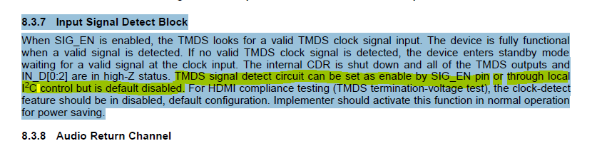
d/s shows that SIG_EN pin can be config by strap pin or I2C.

3. One more question regarding VIH voltage. customer follow TI reference design to use 62Kohm which is near to 65Kohm pull high to 3.3V. customer measure SIG_EN pin voltage, the voltage reduce to 2.5V. could you please provide comment for this?

schematic link

BR,
SHH

  • Scott

    1. Please refer to section 6.5 of the TMDS181 datasheet for the signal condition in standby mode. Does the clock get turned off by the PC in standby mode?

    2. On the schematic, this looks to be a dongle design.
    a. On the DDC, please have TMDS181 unused SDA_SRC and SCL_SRC pulled to GND.
    b. On the DDC between the source connector and sink connector, please add a I2C level shifter to isolate the sink DDC capacitance.
    c. Do they have pullup on EQ_SCL and EQ_SDA?
    d. If the TMDS181 HPD_SRC is connected to the source connector, you may need a 3.3V to 5V level shifter
    e. If HPD is connected directly between the sink and the source connector, you may consider adding a FET switch to isolate the potential sink HPD leakage voltage when sink is off.

    3. The VIL, VIH, and VIM are based upon a microcontroller driving the control pins. The pullup/pulldown/floating resistor configuration will set the
    internal bias to the proper voltage level which will not match the VIL, VIH, and VIM voltage in the datasheet.

    Thanks
    David
  • Hi David,

    thanks for detail. Could you describe how to make sure td3?


    On the DDC, please have TMDS181 unused SDA_SRC and SCL_SRC pulled to GND.

    => if those pin are floating, what impact for this situations?

    On the DDC between the source connector and sink connector, please add a I2C level shifter to isolate the sink DDC capacitance.

    =>customer has a bus repeater within source connector and sink connector. Thanks for your remind.

    Do they have pullup on EQ_SCL and EQ_SDA?

    ==> Yes, the pull up resister put on scalar board.

    If the TMDS181 HPD_SRC is connected to the source connector, you may need a 3.3V to 5V level shifter

    So far, HPD_SRC is floating. But the resister R178 will not use.

    If HPD is connected directly between the sink and the source connector, you may consider adding a FET switch to isolate the potential sink HPD leakage voltage when sink is off. 

    Yes sure, customer put on scalar side.

    BR,

    SHH


  • Scott

    Td3 is an internal timing, it shows that once the retimer mode is enabled, it takes max of 15ms for the CDR to be active.

    Thanks

    David

  • Hi David,

    thanks for help. Are unused SDA_SRC and SCL_SRC  floating ok?

    BR,

    SHH

  • Scott

    Please have SDA_SRC/SCL_SRC connected to GND so noise will not be coupled onto SDA_SRC/SCL_SRC and create an issue with the HDMI operation.

    Thanks

    David