This thread has been locked.

If you have a related question, please click the "Ask a related question" button in the top right corner. The newly created question will be automatically linked to this question.

SN75DPHY440SS: Bit Error

Part Number: SN75DPHY440SS


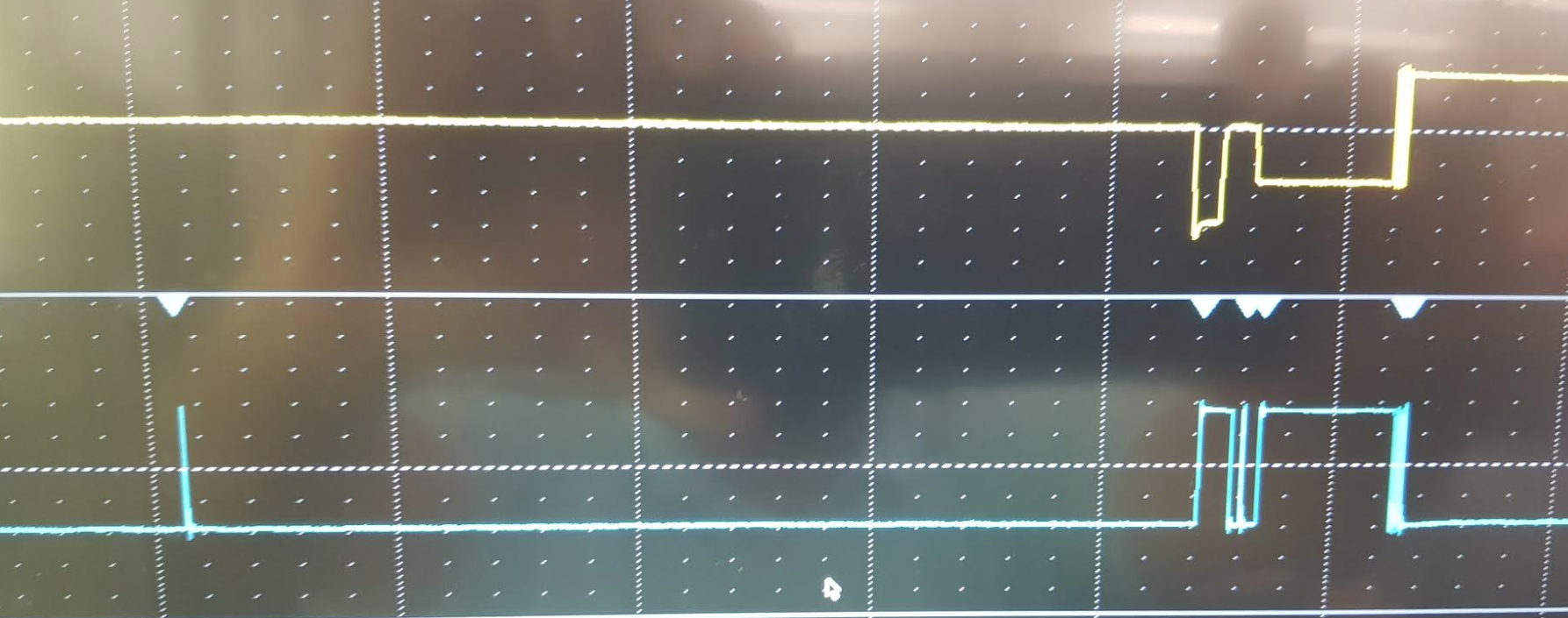
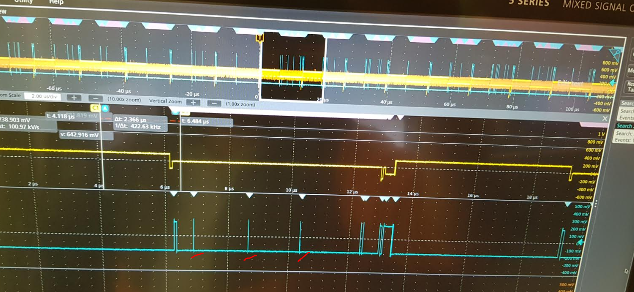
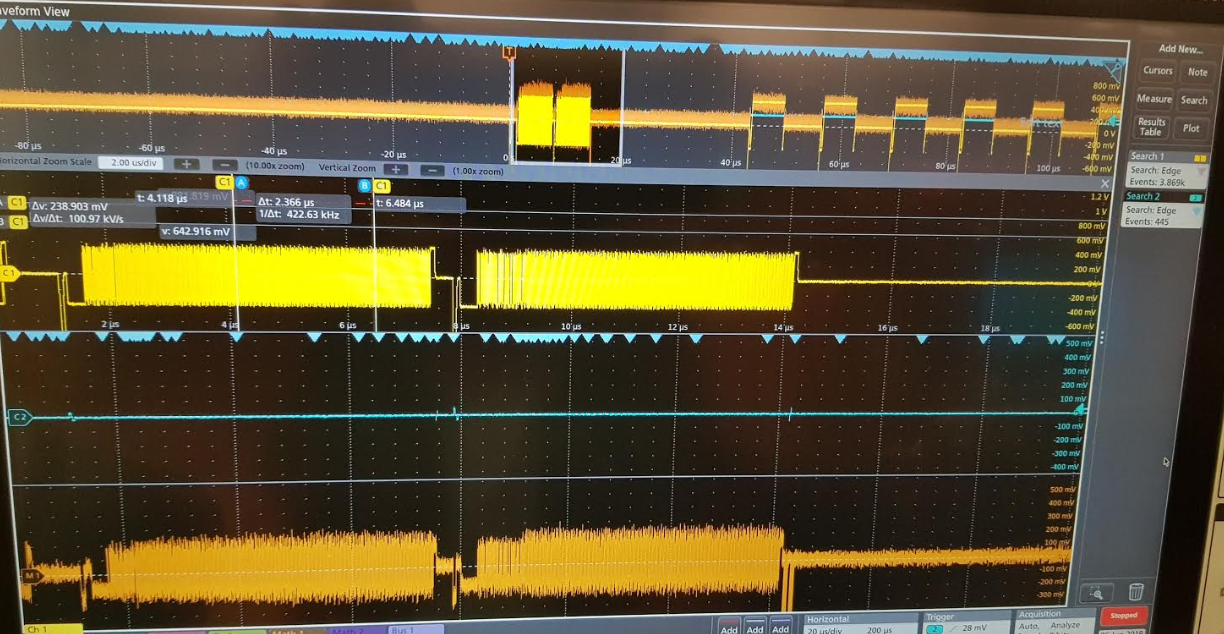
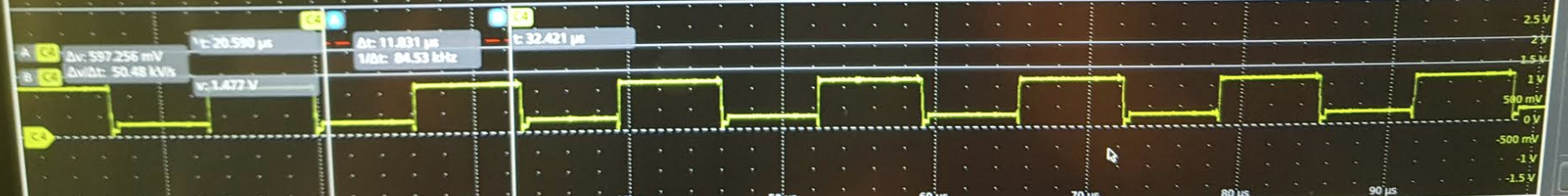
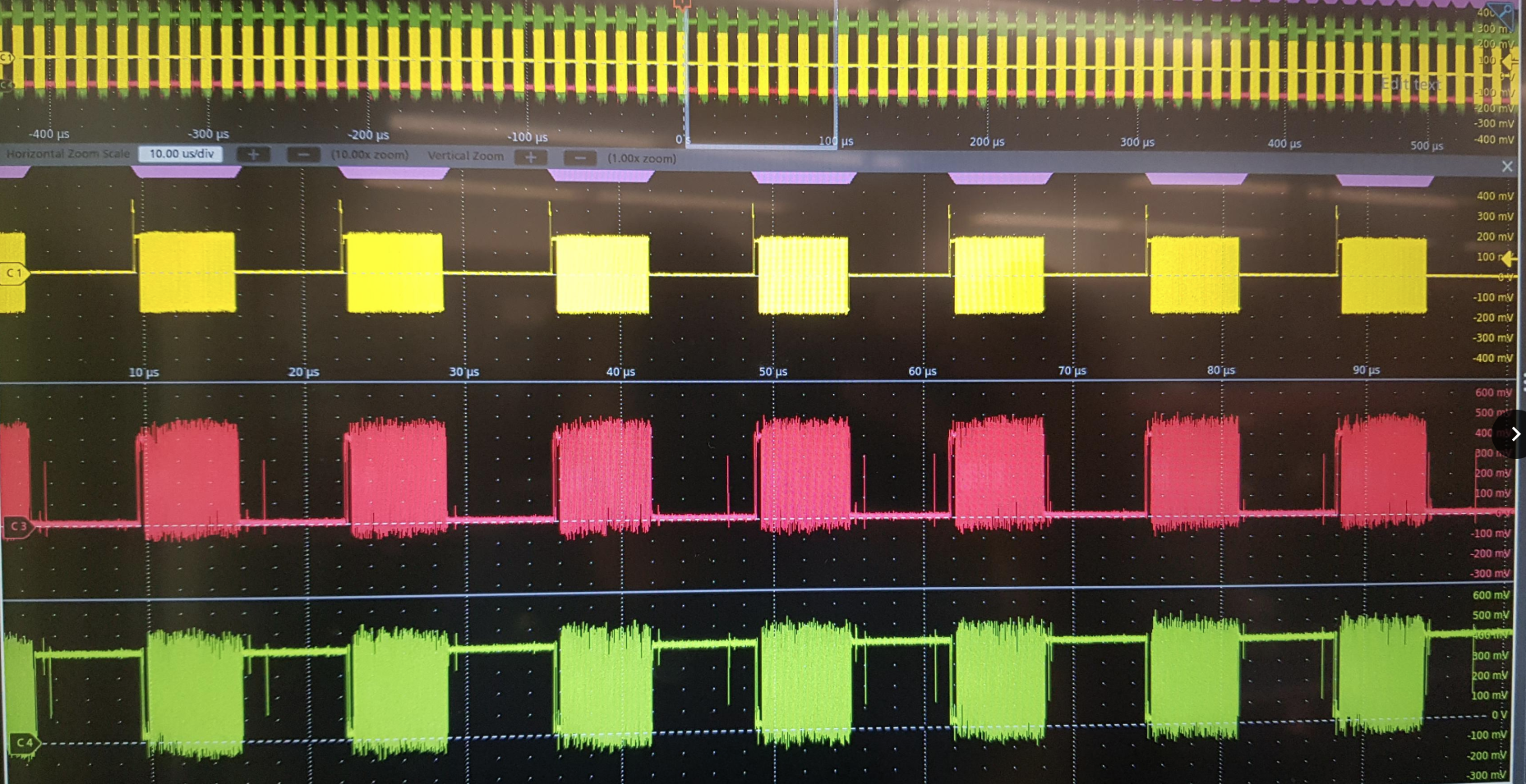
We are seeing some behavior with the chip that we are trying to characterize a bit more, but at a high level it seems to indicate that there is a random pulse being generated on the output side of the chip, which wasn't seen on the input. 

-          Is there any functionality in the device itself, which, after de-skewing incoming signals (with the 2 clock delay), sends out a flag/equivalent start pulse to the output/host? This largely happens on lane 0 pins (1, 2, 23, 24)

-          Is it possible that the de-skew function is causing any unforeseen issues? Is there a way for us to turn it off, and purely use the chip as a re-driver?

-          Is it possible that because lane 0 is a special bi-directional lane for low-power mode, we have to terminate it differently?

Thanks,
Nick

  • Nick

    With Lane 0 path (DA0P/N and DB0P/N) supporting bi-directional LP signaling, it is very important that DB0P/N LP TX is connected to an unterminated LP RX.  If DB0P/N LP TX is connected to a HS RX, then LP signaling will not be able to reach the LP11 levels and which will cause the DPHY440 to not enable HS data path on Lane0.

    You can enable HS path for lane 0 only by the following I2C instruction:

    Enable HS path for Lane 0 only:
    Write Register 0x50 with 8’h01 //Override enable for HS TX path
    Write Register 0x51 with 8’h01 //HS TX path enabled.
    Write Register 0x61 with 8’h00  // Disable LP path.
    Write Register 0x70 with 8’h01  //Override enable for HS RX path
    Write Register 0x71 with 8’h01  // HS RX path enabled.
    Can you please see if this will solve the issue you are seeing?
    Thanks
    David
  • We've implemented the above changes in the past on Lane 0 but not the other lanes, I am wondering if that is causing any cross-talk concerns for us.

    here is the error I am seeing: when I look at the output (blue line in the photo below) of the DPHY440 part, measured at the far end (where it is currently unterminated), I get this on the oscilloscope:

    As you can imagine, this pulse could be caused by a variety of factors. So far I have ruled out termination (all terminations are removed above), power supply voltage noise (there is some noise in the rails, but that is not what is coupling in here), and simultaneous switching output possibilities (newer FPGAs are good about balancing this anyway).

    Currently, among other things, I am also considering noise coupling from the other three diff pair signals that make up the MIPI interface. If this is the case, I was wondering if I could turn off LP path on all lanes. will this be ok from the part's perspective? Anything I should look out for when running in such a configuration?

    Thanks,
    Nick

  • Nick

    For all lanes:
    Write Register 0x50 with 8’h1f //Override enable for HS TX path
    Write Register 0x51 with 8’h1f //HS TX path enabled.
    Write Register 0x61 with 8’h00  // Disable LP path.
    Write Register 0x70 with 8’h1f  //Override enable for HS RX path
    Write Register 0x71 with 8’h1f  // HS RX path enabled.
    Thanks
    David
  • Hi David,

    As suggested, I tried turning LP mode off on all paths. However, it didn't work out, as shown here:

    I then decided to turn LP mode ON on all paths (basically exactly opposite of the settings above); as expected, lane 0 stopped transmitting high speed signals. However, interestingly (and for the first time), I saw the runt pulses actually line up with the event when the input signal actually toggles at LP-mode levels (fyi: new amber signal is neighboring lane 1 TX, which is apparently just chugging along fine, and not being affected by the runt pulses):


    I then wondered what would happen if I only disable LP mode on just Lane 0 (just change register 61 to 0x1E), and I get the following image where the magnitude of the runt pulse seems to decrease (which leads me to think there is some path inside the device that imposes the path on lane 0):


    To surmise, I think there is something turning on/off during the LP-mode to HS-mode transition on the input side, which is somehow bleeding through in Lane 0 of the output side.


    Is there a comprehensive document with all these registers listed, that you can share with us? I am wondering if the dynamic termination on the input side has an effect here. Since lane 0 is the only lane that can be bidirectional, there is some shared line that is feeding back this runt pulse?


    Thanks,

    Nick

  • Nick

    What is channel 0 and channel 1 of the scope?

    Is DPHY440 lane 0 connected to a un-terminated RX?

    Thanks

    David 

  • Apologies on that: 

    Channel 1-> Yellow channel is the Lane0 input to the TI part, as measured at the TI part; Channel 2 -> Blue channel is the Lane0 output of the part, as measured at the far end host's RX pins; Math Channel -> Amber channel is the lane 1 output of the TI part, as measured at the far end host's RX pins

    Is DPHY440 lane 0 connected to a un-terminated RX?: Yes it is; irrespective of terminated/unterminated, we still see these pulses

    Best,
    Nick

  • What is channel 0 and channel 1 of the scope? 

    Channel 1-> Yellow channel is the Lane0 input to the TI part, as measured at the TI part; Channel 2 -> Blue channel is the Lane0 output of the part, as measured at the far end host's RX pins; Math Channel -> Amber channel is the lane 1 output of the TI part, as measured at the far end host's RX pins

    Is DPHY440 lane 0 connected to a un-terminated RX?

    Yes it is; irrespective of terminated/unterminated, we still see these pulses

  • Nick

    The Low power module, an unterminated module, operate in single ended manner and work on 1.2V logic voltage. The high speed, on the other hand, operates in a differential manner. They utilize the low voltage swing of the payload data signals to transfer the information with the typical differential output swing of high speed signals at 200mV.

    If I take a look at Channel 1 waveform, the LP and high speed are almost at the same voltage, so I think we need to understand why the LP is not operating at 1.2V first.

    Thanks

    David

  • Hi David,

    Please note that the vertical scale was zoomed in to about 100mV/division so that only the high speed signals can be captured, and the low power transitions will be clipped. If you look at the top side of the second and third pictures closely, you will see multiple clipped yellow transition to the LP mode. Since we wanted to focus on the portion where our issue starts/ends, we are zoomed in on the HS signal.

    So, to answer your LP question, in the 1st and 3rd picture, we have just turned LP mode OFF, so we wont see the blue line match with the yellow one. And then, in the second picture, I just assumed that since LP mode is enabled, the part will not accept the settings. I would be happy to send you LP mode signaling plots if needed.

    Thanks,

    Rohan

  • Rohan

    Why is the LP below the reference ground? Are you AC coupling the lane?

    Thanks

    David

  • Hi David,

    I am using active diff probes on those lines, so I am forced to DC-coupling.

    However, if you want to take a look at the direct/single ended output of the pins, here is the single-ended FET probe view (DC coupled again, but shows the appropriate Vcmtx of around 210mV, and a swing of about 180mV):

    Also, on another note, I was also able to capture the low power mode single ended output on Lane1 (pins 21 and 22) of the TI part:

    It should be noted that I have not been able to see the Lane 0 (pins 23 and 24) output toggle at LP-mode levels..

    Thanks,

    Rohan

  • Rohan

    Are you seeing the LP going to lane 0 of DPHY440 (pin 1 and 2)?

    Can I take a look at your schematic?

    Thanks

    David 

  • Hi David,

    Yes, I am getting LP mode on the input pins, but no matter what, it doesn't make its way to the output. However, this shouldn't matter because by default TI recommends LP mode to be off any way, right? So, why focus on that?

    As for the schematic, I believe Verb has a NDA with TI, but before I send any proprietary information, I would like to ask what the visibility of this forum is? Because while I may be able to send you the information via email, I am unable to publish it in a public discussion forum, as this one may seem. So please send me an email id for the same.

    Just to give you an idea of the structure, the signals are pretty much routed as though they were point to point. On the input side, they come from a sensor through a connector; on the output side they feed a FPGA, through another connector. I believe the impedance profile of the path far exceeds what is required by MIPI, and I have not seen any signal integrity issues on the high speed path (once communication has been established).

    Thanks,

    Rohan

  • Rohan

    If you are only disabling the LP on lane 0 but keep LP enabled on all other lanes, are you still seeing the bit error?

    Write Register 0x50 with 8’h1f //Override enable for HS TX path
    Write Register 0x51 with 8’h1f //HS TX path enabled.
    Write Register 0x61 with 8’h1E  // Disable LP path.
    Write Register 0x70 with 8’h1f  //Override enable for HS RX path
    Write Register 0x71 with 8’h1f  // HS RX path enabled.
    Can you also use single end probe and capture both lane0_p and lane0_n?
    Thanks
    David
  • Hi David,

    Yes in this case it closely resembles the default case which has settings as:

    Write Register 0x50 with 8’h01 //Override enable for HS TX path
    Write Register 0x51 with 8’h01 //HS TX path enabled.
    Write Register 0x61 with 8’h1E  // Disable LP path.
    Write Register 0x70 with 8’h01  //Override enable for HS RX path
    Write Register 0x71 with 8’h01  // HS RX path enabled.
    I dont have a single ended capture for this, but can send it over in a few minutes..
    Thanks,
    Rohan
  • Hi David,

    Here is the plot for that setting (yellow is diff probe input, red and green are single ended outputs), as you can see the glitch is still present:

    However, since I was in there, I tried a few more settings, and realized that the following settings:

    gave me a very clean output (mostly because the output is now clipped at 1.2V instead of at the diff mode return):

    For our application, elimination of the glitch is of extreme importance. Do you see any concerns with the settings above?

    Thanks,

    Rohan

  • Rohan

    You are enabling LP and clearing all HS enable over-ride on all the DB_P/N path. I do not see an issue with this configuration.

    Thanks

    David  

  • Hi David,

    Are these settings any different from the default ones? Is there a document that lists the registers in this part, and their default values?

    Thanks,

    Rohan

  • there may has default setting, but each application is different. If your setting is clean and working, that's the best setting for your application.

  • Thanks Brian. While I agree, our failures have not gone away, but have reduced clearly. Additional insight into the registers would be very helpful in that regard, hence was asking for the register map. On another note some of our failures can also be attributed to the incorrect mounting of the TI part onto our board. Is it possible to share a thermal profile recommendation for our assembly house to use?

  • Rohan

    Please see this app note for the thermal profile recommendation: http://www.ti.com/lit/an/slua271b/slua271b.pdf.

    Thanks

    David