This thread has been locked.

If you have a related question, please click the "Ask a related question" button in the top right corner. The newly created question will be automatically linked to this question.

PCA9306: VIH/VIL level on SCL1/SDA1 and SCL1/SDA1 on PCA9306

Part Number: PCA9306

Hello support team,

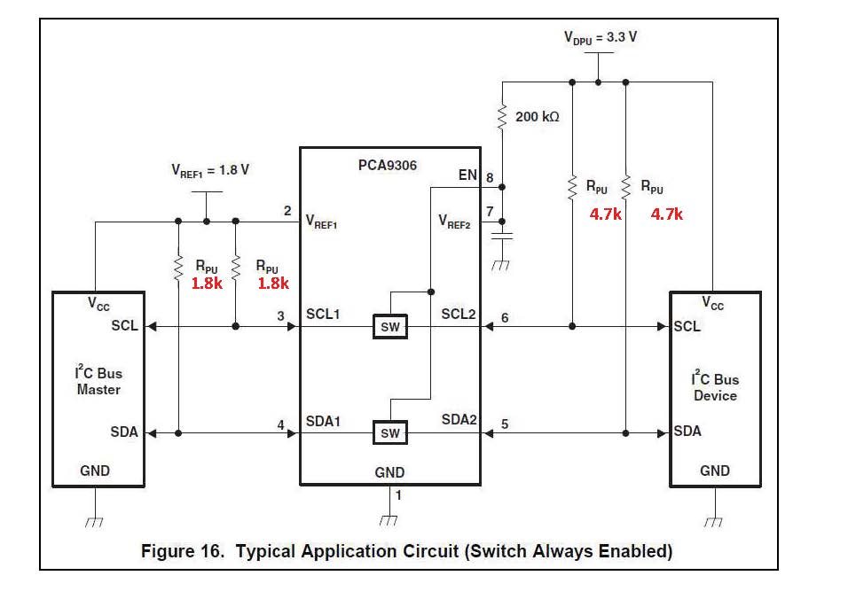
My customer need to know the VIH/VIL level on SCL1/SDA1 and SCL2/SDA2 at the specific condition as follows. Also the circuit configuration is shown in a schematic in below.

- VIH/VIL for SCL1/SDA1

Min VOH at SCL1/SDA1 is 2.31V (Sink Current is larger than 0.21mA)

Max VOL at SCL1/SDA1 is 0.99V (Sink Current is larger than 0.49mA)

How much value is VIH for SCL1/SDA1?

How much value is VIL for SCL1/SDA1?


- VIH/VIL for SCL2/SDA2

Min VOH at SCL1/SDA1 is 1.26V (Sink Current is larger than 0.30mA)

Max VOL at SCL1/SDA1 is 0.54V (Sink Current is larger than 0.70mA)


How much value is VIH for SCL2/SDA2?

How much value is VIL for SCL2/SDA2?


The customer said to follow the internal rule in the company they need to show the value to go the mass production. Otherwise could not go the next step so we need to get your help.


Your help would be very appreciated.


Best regards,

Izumi Maruyama

  • Hello Maruyama-san,

    VIH/VIL specifications are typically defined for a digital input buffer, i.e., a circuit that would take some analog input voltage and resolve it into either a "logic high" or "logic low" state based on these threshold voltages.  The PCA9306 device's SDA/SCL IOs are not digital in nature, though, and instead act like an analog switch.  This device accomplishes level translation by conducting between the signals on sides "1" and "2" whenever the voltage on either side decreases below the VREF1 level.  For voltage levels of VREF1 or higher, the conduction is blocked - this allows for a larger high-level voltage to be pulled up on side 2.

    Because of this design, the low-level voltage that is driven by the device on one side of the PCA9306 will also appear on the other side of the PCA9306.  (Note that the voltages on either side will be very close but may not be exactly the same - there will be an offset voltage introduced by the current flowing through the switch multiplied by the series resistance of the switch.)  The high-level voltages on each side are just set by the pull-up voltages used on each side (minus any voltage drop across the pull-up resistances due to pull-down leakage currents that may be present on the PCB).

    Please let us know if this explanation is not clear to you.

    Regards,
    Max Robertson

  • Izumi-san,

    "VIH/VIL for SCL1/SDA1"

    This device uses a pass FET architecture. This means ViL is essentially ViH. The point at which we will see this is around Vref1.

    "Min VOH at SCL1/SDA1 is 2.31V (Sink Current is larger than 0.21mA)"

    This is I2C, VoH is whatever the pull up resistor is tied to which is why VoH is typically not spec'd.

    "Max VOL at SCL1/SDA1 is 0.99V (Sink Current is larger than 0.49mA)"

    This uses a pass FET architecture, if we decided to use section 6.5 RON of the datasheet then our maximum value is 32 ohms. if you have 0.99V and RON is 32 ohms with a 0.49mA drive then you would see: 0.99V+32*(.000049) = 0.991558V. At this reference voltage and current I would expect the RON to be much lower anyways (around 5 ohms) so VoL would be much lower.

    "How much value is VIH for SCL1/SDA1?

    How much value is VIL for SCL1/SDA1?"

    Like I discussed earlier, ViH=ViL=Vref1

    "VIH/VIL for SCL2/SDA2"

    See above

    "Min VOH at SCL1/SDA1 is 1.26V (Sink Current is larger than 0.30mA)"

    1.26V is below Vref1 so it would be around 1.26V

    "Max VOL at SCL1/SDA1 is 0.54V (Sink Current is larger than 0.70mA)"

    0.7mA is incredibly low, you would see 0.54V on the other side.... (See my math above for the other case).

    "How much value is VIH for SCL2/SDA2?"

    ViH=Vref1

    "How much value is VIL for SCL2/SDA2?"

    ViL=Vref1

    -Bobby


  • > For voltage levels of VREF 1 or higher, the conduction is blocked-this allows for a large high-level voltage to be pulled up on side 2.

    There was a description.
    When a voltage higher than VREF1 is applied, the connections (1 side and 2 side) are blocked, so the output logic becomes HiZ and the output voltage becomes Hi under the influence of pull-up,
    I understood that.

    On the other hand, if the pull-up voltage on the SCL1 and SDA1 side is the same as Vref1, I think that it is impossible to make these input voltages literally higher than Vref1.
    It is presumed that there is probably a lower limit value such that the voltage of SCL1 and SDA1 is “more than ○○% of VREF1” or “more than ○○ V”.
    Could you tell me about the conditions?
    (For example, if the voltage of SCL1 and SDA1 is 99% of Vref1, does it correspond to "the conduction is blocked"? Also at 98%? 90%? )

  • Hey Yoshihiko,

    "It is presumed that there is probably a lower limit value such that the voltage of SCL1 and SDA1 is “more than ○○% of VREF1” or “more than ○○ V”.
    Could you tell me about the conditions?
    (For example, if the voltage of SCL1 and SDA1 is 99% of Vref1, does it correspond to "the conduction is blocked"? Also at 98%? 90%? )"

    The further below you go under the Vref1 voltage, the more conduction occurs. I would say, if side 1 (SDA1/SCL1) goes below Vref1 by ~0.4V then we will see conduction occur (higher temps make this conduction occur sooner and lower Vref1s make conduction occur sooner). The lower you go, the stronger the conduction becomes. The conduction is a linear function of the difference between side 1 and Vref1 voltages. (Being below by 1V will be twice as strong as being below by 0.5V).

    -Bobby

  • Hi Bobby!

    ● Confirmation 1
    I understood this, is it correct?
    ---
    Assuming that the voltage drop at 200 kohm is negligibly small, let Vref2 be 3.3V.
    In order to make side 2 2.31 V, it is necessary for conduction (conduction) of 3.3 V-2.13 V = 0.99 V.
    
    Conduction [V] = Vref1 [V] / side1 [V]
    Conduction = 0.99
    Vref1 = 1.8
    Solve for side 1
    side1 = 0.55
    
    Thus, if side1 is greater than or equal to 0.55 V (at a certain temperature), it is guaranteed that side2 is greater than or equal to 2.31 V.
    ー
    
    ● Confirmation 2
    > higher temps make this conduction occur sooner
    For example, how much does it change at 0 ° C, 25 ° C, and 50 ° C?
    Five %? Ten%? Is it smaller?

  • "Conduction [V] = Vref1 [V] / side1 [V]"

    The conduction voltage is not a percentage, it is a value that varies across temperature and doping levels. Typical I would say is around ~0.6V at room temperature though I would use 1V as a maximum value (most likely you won't see it this high).

    "● Confirmation 1"

    If you pulled side 1 to 0.55V then side 2 would be slightly larger than 0.55V (Maybe 0.6V, depends on the load current). 

    "● Confirmation 2

    > higher temps make this conduction occur sooner For example, how much does it change at 0 ° C, 25 ° C, and 50 ° C? Five %? Ten%? Is it smaller?"

    This kind of data is not catalogued, If you need an estimate you could likely get this estimate by looking at a few diode Vforward versus Temperature. Google search tells me that it could be around 30% lower at very high temperatures (125C) but its starting point depends on the load current. Lower load currents provide a lower Vforward. graphs seem very linear.  At ~75C the percent change is likely around 15%. At 50C this change is likely around 7.5%. Again with a 25C change (referenced to 25C) then 0C should show a 7.5% increase from 25C. These would be my estimates based on general diode behavior.

    -Bobby