This thread has been locked.

If you have a related question, please click the "Ask a related question" button in the top right corner. The newly created question will be automatically linked to this question.

DP83620: DP83620 EMC TEST Issue

Part Number: DP83620

Hi Team, 

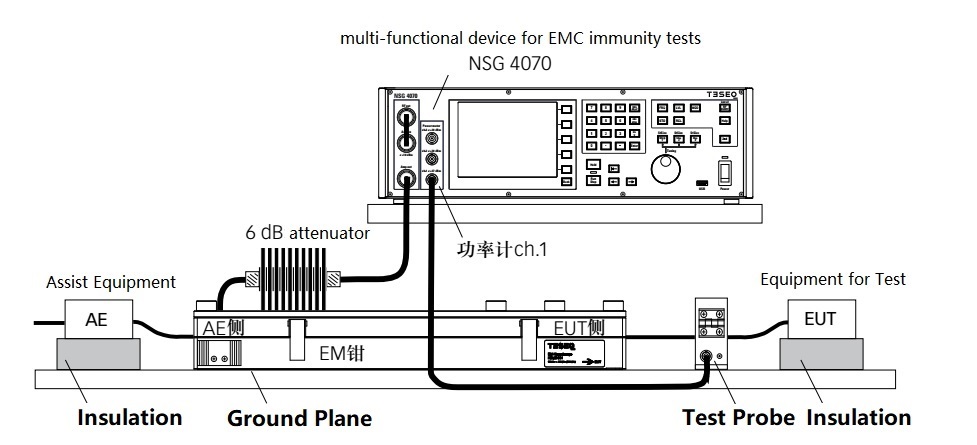
My customer is doing the design with DP83620 with RMII mode. When they do the EMC test with some frequency wave form(RMS=10V) as below: they found that, if the frequency is set to 50Mhz-60MHz, the DP83620’s communication would be lost sporadically. If setting the 51MHz as the test frequency, the dp83620 would always fail with Ethernet communication.

By contrast, they did the same test on two other Ethernet port, one is DM9000, the other is Intel I210. See PCB for the position and layout. But there’s no issue with those two expanded Ethernet ports.

So they’d like to learn whether there are some approach could help to improve the EMC test performance?

  • Hi Steven,

    Please share the schematic and layout of the board they are using.

    EMC performance is very layout dependent.

  • Hi Ross,

    Thanks for your reply on this. An email was sent to you with the SCH and PCB due to the confidentiality.

    Please feel free to give your comment on this! Many thanks for the support! 

  • Hi Steven,

    Thank you for the layout.

    There are serious issues with the MDI routing.

    1) I see no track route matching between the plus and minus lines. There is over 15% mismatch between the differential lines.

    2) I see a via where the MDI is split to two different connectors. This is a massive stub that most certainly is going to cause emission and immunity issues.

    3) Sig1 and Sig2 have no ground between them.

    4) VCC is a mixture of power and ground. This is the nearest ground reference for Sig2 and a few of the signal routing on that layer do not have a solid ground reference because power routing is cutting them. 

    5) I see metal pours between differential routing pairs.