


Part Number: SN65DPHY440SS
Hi team,
My customer is designing the SN65DPHY440SS schematic. Please see below picture. I already checked it and didn't find anything wrong. But hope you could also double check on it. Thanks.
Best regards,
Wayne
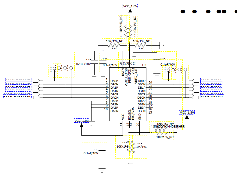
Part Number: SN65DPHY440SS
Hi team,
My customer is designing the SN65DPHY440SS schematic. Please see below picture. I already checked it and didn't find anything wrong. But hope you could also double check on it. Thanks.
Best regards,
Wayne
