This thread has been locked.

If you have a related question, please click the "Ask a related question" button in the top right corner. The newly created question will be automatically linked to this question.

TCA9617B: Does TCA9617B input comes with internal Schmitt?

Part Number: TCA9617B
Other Parts Discussed in Thread: TCA9517

Hi,

i'm looking into datasheet of TCA9617B & still determining if this device is suitable for my system and I have questions which needs verfication.

Does TCA9617B carry built-in Schmitt Trigger on it's input pins? 

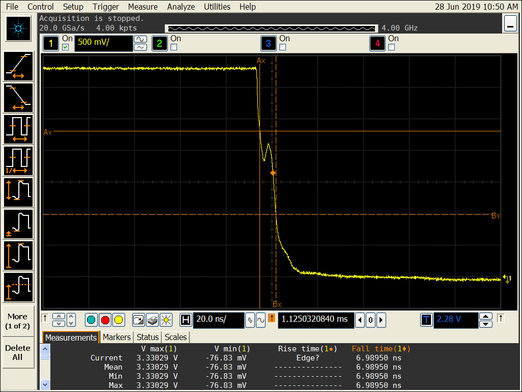
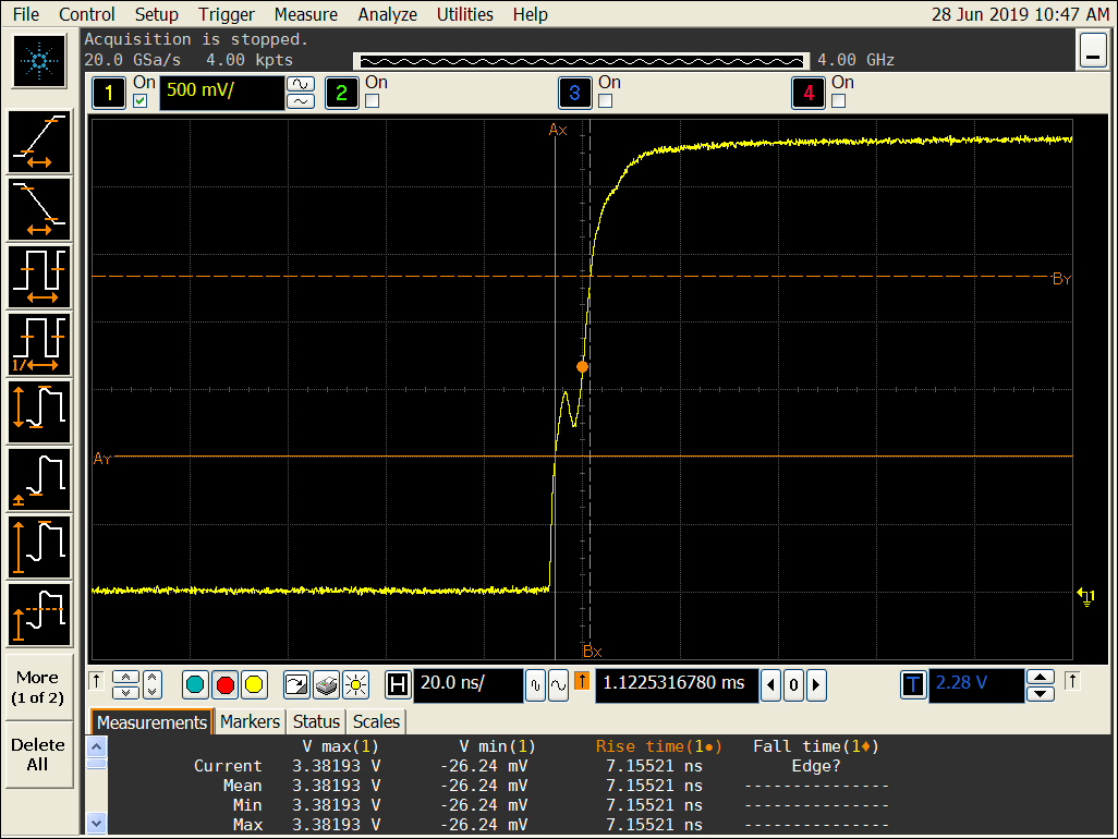
In my use case I'm having a non-monotonic I2C clock and data signal inbound and i'm concerned if this might cause double-triggering in my system.

Also if there's indeed schmitt triggers on the input pin, what are the V+(Upper Trip Point) and V-(Lower Trip Point) ?

  • Hey Leo,

    This device does have schmitt triggers/hysteresis.

    I tried to mess around and find the values in the design file but I ran into quite a few hiccups. I'll try to put it on the bench tomorrow and get back to you but my initial thoughts are below:

    B side should have a lower input value of ~400mV and releases at ~500mV.

    For A side there should be atleast 0.05*VccA for a hysteresis value (I2C spec) my guess here is probably 10%. The devices begin looking for a low input slightly above the 30% of VccA value spec'd in the datasheet inorder to meet all corners. Worst cause in this assumption should be V-=30% and V+= 40% to V-=35% and V+ = 45%.

    -Bobby

  • Leo,

    What I saw on the bench for the ViL for A side was around 33% VccA and the hysteresis looks like it only has around 20mV of hysteresis so my initial thoughts were wrong (post above).

    For B side I was not able to run the test due to my power supply latching to 600mV. I do believe my original post above about the ViLB and release point are correct however (TCA9617B uses similar design as the TCA9517 so I believe this to be correct.). If you need verification on this, I can run into the lab to double check this (let me know).

    -Bobby

  • Hi Bobby,

    I'm attaching a screenshot whereby client probed at the TCA9617B's A side.  They are non-monotonic edge at the falling edge. Does the V-, V+ for the falling edge are also same as the V- and V+ for rising edge?


    I re-attach the rising and falling edge of the I2C clock signal (probed at A side) below. Could you please advise would the observed non-monotonic edge potentially cause false triggering?

    Also for the assumption you made on earlier post, it actually no characterized & recorded in datasheet correct?

    Regards,

    Leo

  • Hi Bobby,

    as attached. Thanks.

  • Hey Leo,

    The rising and falling V+ V- thresholds are the same.

    "I re-attach the rising and falling edge of the I2C clock signal (probed at A side) below. Could you please advise would the observed non-monotonic edge potentially cause false triggering?"

    The width of the glitch looks incredibly small, sub 5ns? That likely isn't enough time for the logic to propagate through our device. The glitch is smaller than ~5% of the propagation delay from A to B side.

    I don't think that's enough time for the input stage's FETs to turn on in time even if it was at the hysteresis +/- values.

    "Also for the assumption you made on earlier post, it actually no characterized & recorded in datasheet correct?"

    That's correct. I looked in our internal database to see if I could find data on the hysteresis points but did not find anything on it.

    -Bobby