This thread has been locked.

If you have a related question, please click the "Ask a related question" button in the top right corner. The newly created question will be automatically linked to this question.

SN65DP159: Schematic review

Part Number: SN65DP159

Hi Sirs,

Sorry to bother you.

Could you help double check our schematic as below? Any suggestion are welcome.
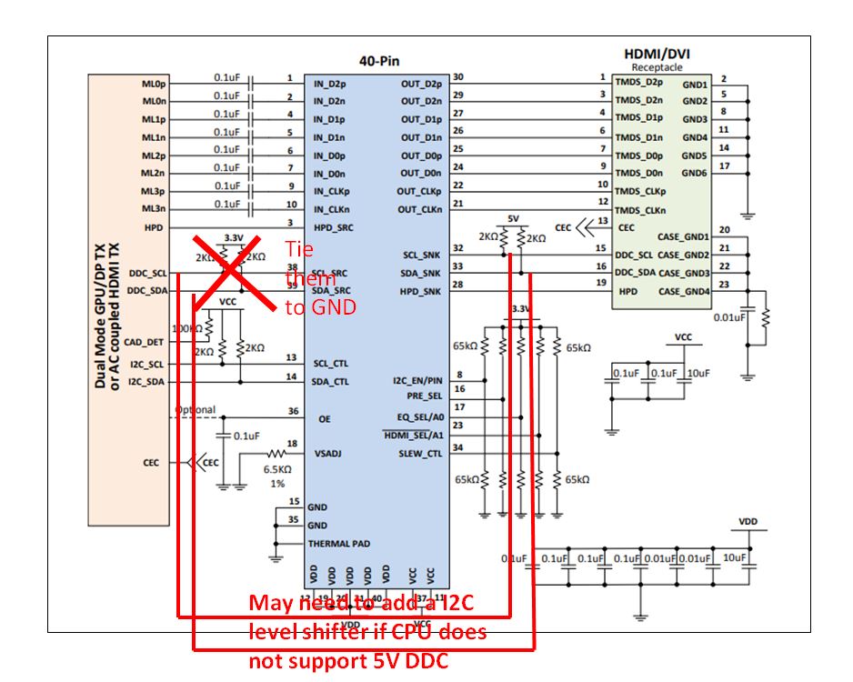
Schematic:

Some question need confirm too.

1) I set to use Strap Pin to adjust the setting. Are SCL_CTL / SDA_CTL I2C I/F can be floating? (No Pull up)

2) But I also reserve the possibility to connect the above I2C to PCH I2C to let the BIOS set this HDMI IC. At this time, those Strap pins, for example, can be double-selected by Strap pin or I2C.
For example, how to connect SLEW_CTL Pull up/down

EQ_SEL, HDMI_SEL also set I2C Address, will set the top pull up / down
Other I2C_EN, TX_TERM_CTL has other functions or has the upper piece Pull up/down

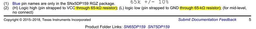
3) Strap pin should use 65K ohm resistor, but this resistor value not in our internal parts pool. So what is the allowable range of resistance values?

  • Shu-Cheng

    1. I would pull SDA_CTL and SCL_CTL up to 3.3V through 100k resistor when not being used.

    2. When in I2C mode, they can left floating

    3. 65k pullup resistor tolerance

    [3-Level Input pins]
    Pull-up: 65k +/- 10%
    Pull-down: 0 to 65k + 10%

    [2-Level (LVCMOS) Input pins]
    Pull-up: 0 to 65k + 10%
    Pull-down: 0 to 65k + 10%

    On the schematic, the SNx5DP159 uses clock stretching for DDC transactions. As there are sources and sinks that do no perform this function correctly a system may not work correctly as DDC transactions are incorrectly transmitted/received. To overcome this a snoop configuration can be implemented where the SDA/SCL from the source is connected directly to the SDA/SCL sink. The SNx5DP159 will need its SDA_SNK and SCL_SNK pins connected to this link in order to the SNx5DP159 to configure the TMDS_CLOCK_RATIO_STATUS bit. Care must be taken when this configuration is being implemented as the voltage levels for DDC between the source and sink may be different, 3.3 V vs 5 V. The SDA_SRC and SCL_SRC must be tied to ground.

    Thanks

    David

  • Hi Sirs,

    Thanks for your reply,

    For item 3, this is scary me.

     Datasheet sn65dp159 2018_05 version page 5 specific the pulls resistor through 65K ohm.

    But some reply say 65K + 10% ONLY, no negative tolerance?

    So my 64.9K ohm pulls resistor is not valid?


    [3-Level Input pins]
    Pull-up: 65k +/- 10%
    Pull-down: 0 to 65k + 10%

    [2-Level (LVCMOS) Input pins]
    Pull-up: 0 to 65k + 10%
    Pull-down: 0 to 65k + 10%


    And you mention below note, not clear.

    So you want to do these modification?

    1)      Not use SN65DP159 DDC isolator (CPU 3.3V to HDMI 5V level signal isolator

    2)      Design external CPU 3.3V to HDMI 5V level signal isolator.

    3)      But still connect SN65DP159 SDA_SNK/SCL_SNK pin to HDMI port

  • Shu-Cheng

    This is a typo on my part, the tolerance is 65k +/- 10%.

    Please see the block diagram for the DDC connection. 

  • Hi Sirs,

    Thanks for your reply,

    The DDC channel connection modify is clear.

    But why to do this?

    I already modify the schematic
    Please confirm again, thanks.

    1. Add DDC isolator/level shifter circuitry
    2. Change Strap pulls resistor value

    Schematic:

  • Shu-Cheng

    The schematic looks OK.

    Thanks

    David