


Part Number: DS90UB914Q-Q1
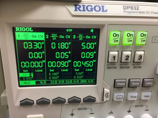
914Q and 913Q link without LOCK signal, PASS signal 1. Confirm that 913Q is OK and that the link between 913Q and 914Q is LOCK signal. 914Q peripheral circuits and capacitance matching are patched according to specifications. We did the following experiments 1 PDB signal is controlled by RC10K resistance 10UF capacitor patch, which is invalid. Manual pull-up 3.3V level is also ineffective 2 MODE mode also operates separately according to 0 ohm 3K 11K resistance, which is also invalid. 3 ID1 ID2 pull-up all 10K pull-down all 0 ohm invalid SEL level set to 0, BISTEN level is 0 OEN pull-up 3.3V OSS_SEL pull-up 3.3V The RIN0 channel is used. 4. We supply VDDIO and VCC1V8 power respectively with DC power supply, but we still can't LOCK. The current consumption part is shown in the figure. The 914Q part of VDDIO current should be less than 10ma, the accuracy of power meter is not enough to display only 10 bits. The current consumption of VCC1V8 is 50ma. 913Q partial current consumption is 90mA
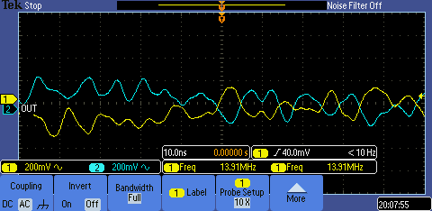
913Q is set to use PCLK. When there is no PCLK, the RIN0 signal is shown in the figure. 914Q Capacitor Terminal Graphics
913Q initializes the sensor, outputs 8M PCLK from sensor, and DATA has signal output. The PCLK of 914Q has no output. No LOCK. I2C reads 914Q registers and can read default values normally, but it can not read ser ID values. 913Q has no relationship with 914Q. The schematic diagram is attached. PCB Part We layout with two layers, RIN0 signal transmission and reception path differential without impedance. Wire links between the two boards are shown in the figure.

