This thread has been locked.

If you have a related question, please click the "Ask a related question" button in the top right corner. The newly created question will be automatically linked to this question.

SN65DSI86: DSI86 REFCLK Setting

Part Number: SN65DSI86
Other Parts Discussed in Thread: TEST2

Dear Sir,


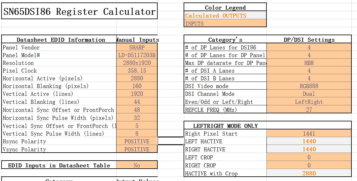
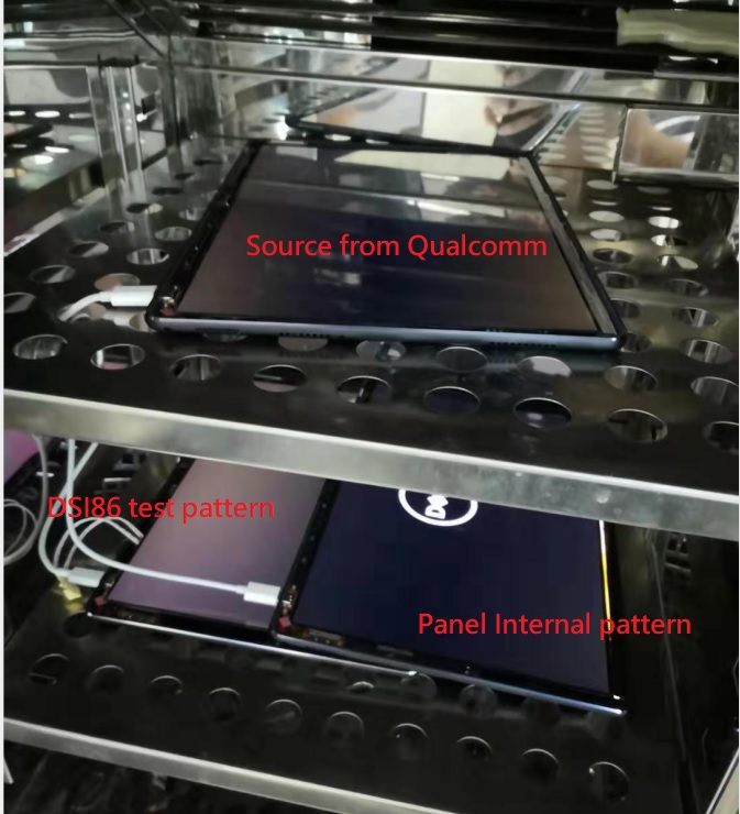
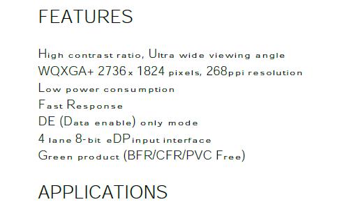
We had new Panel as below( 2736*1824*24bpp*60fps), Does DSI86 support it?

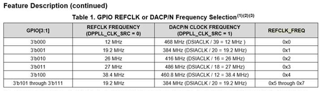
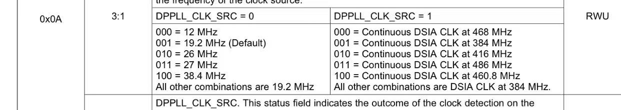
We DSIA_CLK is 520MHz, I saw the SPEC don't have this Freq.
If we use REFCLK  which one Freq can for this Panel
If we use DACP/N CLK, how to chose it?

  • Vincent

    DSI86 can support this resolution. Please accept my friendship request and I will send you a spreadsheet that can be used to calculate the DSI86 registers programming value.

    Thanks

    David

  • Vincent

    I sent you the spreadsheet, please check.

    Thanks

    David

  • Hi David,

    We also have some questions as below

    1. About register 0x0A, Can configure it through DSI? I found this configuration in Qualcomm_noASSR.
    2. About ASSR : I see a description in the document: Because the SN65DSI86 is a DSI to eDP bridge,
    The SN65DSI86 only supports eDP panels which support ASSR (Alternate Scrambler Seed Reset).
    Is ASSR mandatory? Do we need this for our panel?
    3. We use double dsi, left and right screens. How should we configure the parameter Right Pixel Start?
    I guess this: 2736/2 = 1368. Right Pixel Start is 1369, is it right?
    4. Have test pattern in DSI86? We don't have see it in datasheet
    5. How to setting the LEFT CROP and RIGH CROP?
    6. Have any issue in optimum Datarate when I choose HBR?
    We think the calculation process is as follows:
    The pixel Clock of the Samsung screen is 334.9 MHz.
    Stream Bit Rate = 334.9 * 24 = 8.037
    EDP Total Bit Rate = 4 * 2.7 Gbps * 0.8 = 8.64 Gbps
    8.037 < 8.64, So we choose HBR.
    7. Could you help us to check the Calc Spreadsheet?
    Thanks

  • Vincent

    1. You can use DSI to configure DSI86 CSR. When used to configure the DSI86, all communication from the DSI86 to the GPU (read responses) will use DSI channel A lane 0 in LP signaling mode. But I would recommend using the I2C to access the DSI86 CSR since the I2C is always available.

    2. You can disable ASSR by pulling TEST2 pin high, and then execute the 4 lane code in question 1 to disable ASSR control

    3. Right pixel start is 1369

    4. Please refer to the color bar pattern in register 0x3Ch.

    5. LEFT_CROP and RIGHT_CROP are both set to 0

    6.The calculation looks correct.

    7. Attached is the example configuration script file based on the Samsung EDID info with color bar enabled.

    <DSIInitSequence> 
    23 FF 7 \n 
    23 16 1 \n 
    23 FF 0 \n 
    23 0A 2 \n 
    23 10 80 \n 
    23 12 64 \n 
    23 13 64 \n 
    23 94 E0 \n 
    23 0D 1 \n 
    FF 0A \n 
    23 5A 4 \n 
    23 93 20 \n 
    23 96 0A \n 
    FF 14 \n 
    23 20 58 \n 
    23 21 05 \n 
    23 22 58 \n 
    23 23 05 \n 
    23 24 20 \n 
    23 25 07 \n 
    23 2C 20 \n 
    23 2D 00 \n 
    23 30 05 \n 
    23 31 00 \n 
    23 34 8C \n 
    23 36 39 \n 
    23 38 30 \n 
    23 3A 02 \n 
    23 5B 0 \n 
    23 3C 17 \n 
    23 5A 0D \n 
    </DSIInitSequence> 


    Thanks

    David 

  • Hi David,

    1. We want to seeting the test pattern. Can you provide a configuration for it?
    1) In the previous configuration, DP Lane configuration 0x93 is 0x20. Should we need configuration to 0x30 (4lanes)?
    2) I tried to modify the value of the 0x3C register to 10, but it didn't work.
    3) Could you help us configuration it for this test pattern?
    2. 0xFF does not need to be configured, right?
    3. How to choose the ML_TX_MODE when we want to test pattern?
    4. Can we set the 0x5C register to 0x01, if we don't need HPD functionality?
    5. How to configure to read EDID and DPCD, If we use AUX to read EDID and DPCD?
    6. We had configured register DP_PLL_LOCK  to 1, but we read it don't 1, Is this the reason why don't have test pattern? What causes DP_PLL_ENABLE to be set at 1 but DP_PLL_LOCK is not 1?
    7. About hfp, hbp, hori. sync width, vfp, VBP value, do these values DSI and DP need the same?
  • Vincent

    1. We want to seeting the test pattern. Can you provide a configuration for it?
    *** The previous script I sent to you already have the color bar enabled.
    1) In the previous configuration, DP Lane configuration 0x93 is 0x20. Should we need configuration to 0x30 (4lanes)?
    *** Please refer to the DSI86 programming app note: http://www.ti.com/lit/an/slla425/slla425.pdf.

    To calculate the minimum number of eDP lanes you must satisfy the equation below. For example, if the EDP_Total_Bit_Rate = 4.7 Gbps and the eDP_Daterate_Supported = 2.43 Gbps then the minimum number of EDP_Lanes is 2.

    eDP_Datarate_Supports >= (eDP_Total_Bit_Rate / eDP_lanes)

    2) I tried to modify the value of the 0x3C register to 10, but it didn't work.
    *** Please dump out the entire DSI86 registers
    3) Could you help us configuration it for this test pattern?
    *** Color bar is already enabled in the script, which test pattern are you referring to?
    2. 0xFF does not need to be configured, right?
    *** 0xFF is not the DSI86 I2C address
    3. How to choose the ML_TX_MODE when we want to test pattern?
    *** You can use semi-auto link training.
    4. Can we set the 0x5C register to 0x01, if we don't need HPD functionality?
    *** If the eDP panel does not support HPD, it can be disabled.
    5. How to configure to read EDID and DPCD, If we use AUX to read EDID and DPCD?
    *** Please refer to section 8.4.5.3. SW can obtain the DPCD information by using the Native Aux Registers. The eDP panel capability is located at DisplayPort Address 0x00000 through 0x0008F. When reading the DPCD capability, SW needs to be aware that Native Aux transactions, like I2C-Over-Aux, is limited to a read size of 16 bytes. This means SW must read the DPCD in 16-byte chunks.
    6. We had configured register DP_PLL_LOCK  to 1, but we read it don't 1, Is this the reason why don't have test pattern? What causes DP_PLL_ENABLE to be set at 1 but DP_PLL_LOCK is not 1?
    *** This depends on your reference clock frequency and DSI86 programmed value. But PLL needs to be locked.
    7. About hfp, hbp, hori. sync width, vfp, VBP value, do these values DSI and DP need the same?
    *** hfp, hbp, hori. sync width, vfp, VBP value are programmed base on the panel EDID information. We are trying to get the color bar to work for now, so we can ignore the DSI interface programming for now.
    Thanks
    David

  • Hi David,

    We can't output test pattern in DSI86 now. There is no error mark in IRQ status register.           
    All the registers dump out are correct. PLL Lock is successful.          
    How to check this issue? (All registers without error messages)?

  • Vincent

    Would you please dump out register 0xF0h through 0xF8h? 

    Does the panel support the ASSR? If not, do you have the TEST2 pin pulled high?

    Thanks

    David

  • Hi David,

    Could you give me a example for this SHARP’s panel 2880 * 1920 include EDID

    We don’t sure how to input the "Main_Inputs_Page"

  • Vincent

    Please follow the instruction in the first page of the spreadsheet. You use the EDID format page to input the EDID info, and then copy and paste into the main input page.

    Sharp_PANEL_VIDEOREGISTER_CALC.zip

    Thanks

    David

  • Hi David,

    We can show the test pattern in SHARP panel now.
    Before we also can MIPI to eDP in Samsung panel.
    We use the same MIPI setting only change the resolution and DSI CLK in Qualcomm.
    The DSI CLK is 565 MHz, so we change the DSI86 0x12 and 0x13 to 71.
    But can't work.

    Error as below

    F0 01
    F1 2F
    F6 42

    Could you help us to check this issue?

  • Hi David,

    We can show the test pattern in SHARP panel now.
    Before we also can MIPI to eDP in Samsung panel.
    We use the same MIPI setting only change the resolution and DSI CLK in Qualcomm.
    The DSI CLK is 565 MHz, so we change the DSI86 0x12 and 0x13 to 71.
    But can't work.

    Error as below

    0xF0 01
    0xF1 2F
    0xF6 42

    Could you help us to check this issue?

  • Hi David,

    We can output the test panel in SHARP panel now.
    But we can't output from MIPI input.
    Before we use the Samsung panel and use the same platform (Qualcomm), it can output from MIPI input.
    We use the same MIPI setting, change the MIPI Resolution and Pixel Clock for SHARP panel.
    The DSI CLK is 565.63MHz, we had change the DSI86 register 0x12(DSIA Clock) and 0x13(DSIB Clock) to 71.
    But it can't output.
    Could you help us to check it? below is error status, thanks!

    F0 01
    F1 2F
    F6 42

  • Vincent 

    Are you using both DSI channel A and B?

    Instead using the Samsung MIPI setting, can you please using the MIPI setting in the spreadsheet I sent to you yesterday as long as the spreadsheet DSI input condition matches with your hardware DSI configuration? 

    Thanks

    David

  • Hi David,

    Yes, we use both DSI channel A and B.

    Below is our setting, about the hardware, it is only change the panel.

  • Vincent

    Could you please dump out the entire DSI86 register for me to review?

    Thanks

    David

  • Hi David,


    We can display the panel now.

    But we have two problems as below.
    1. Boot-up display screen is placed for a period of time. After a period of time, only have the backlight but not have displayed.
    2. There is a probability that the screen will not wake up if it is repeatedly turned on or off. (SamSung and Sharp have the same issue)

    For the probabilistic wake-up problem, the software reset is executed. Then the initialization I2C configuration is executed. The screen can be displayed.
    Test pattern have the same issue.

    Could you help us to check it?

  • Vincent

    For #2, does the DSI86 gets turned off as well?

    You can try to add a line of code here to see if it helps

    ======Start Semi-Auto Link Training ======

    <i2c_write addr=0x2D count=1 radix=16> 96 02 </i2c_write> <sleep ms=20/>

    <i2c_write addr=0x2D count=1 radix=16> 96 0A </i2c_write> <sleep ms=20/>

    Assuming the issue is related to the link training, the other option is to change the pre-emphasis and SWING level in the DP Link Training LUT registers.

    If the panel supports fast link training, you can change the DP main link training from semi-auto training to fast link training. Please see section 8.4.5.7.2 for detail on the fast link training.

    Thanks

    David

  • Hi David,

    What conditions DP_PLL will from lock to unlock?

  • Vincent

    Please probe the clock at the DSI_CLK or the REFCLK input and make sure the clock is within the DSI86 PLL requirement.

    Thanks

    David

  • Hi David,

    We put the set in temperature chamber.
    The panel don't have display when DSI86 about 72°C.
    We have use the panel Internal pattern is OK, DSI86 use test pattern still is fail.
    Could you help us to check this issue?

    We read the 0xF4 is 41

    How to check the status from EDID?
    How to fill in the AUX_ADDR?

  • Vincent

    The DSI86 reported I2C-over-AUX or native AUX failure.

    Can you please read the EDID and see if the EDID you read match with the panel EDID info?

    To read the EDID, please follow the procedure in section 8.4.5.3

    Thanks

    David

  • Vincent:

        Can you read EDID?

    Brian