This thread has been locked.

If you have a related question, please click the "Ask a related question" button in the top right corner. The newly created question will be automatically linked to this question.

P82B96: Down-spike on the SCL line when SDA enters start condition

Part Number: P82B96
Other Parts Discussed in Thread: TCA6424A, LM2596

Hi!

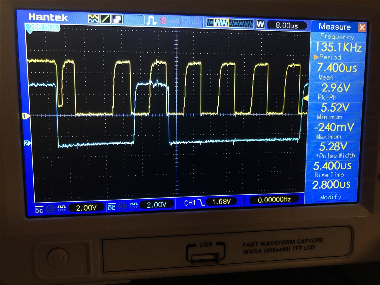
I am having a strange down-spike on the SCL line at the same time the SDA line enters start condition. Please, have a look at the picture.

My original set-up is one I2C master (Raspberry PI) with one slave (MCP23017) and P82B96 on the master board and 4 slave boards connected in a star topology with ca 10 m CAT6 cable per branch. Each slave board has its own P82B96 and MCP23017. I also used logical level convertor on the master side (3.3V/5V).

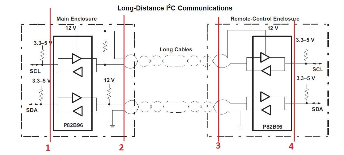
Due to the above problem I reduced the set-up for troubleshooting and now it boils down to this standard diagram:

The cable has moderate length of about 5-7 m and it is CAT6.

If I connect the slave board directly to I2C master (Raspberry PI) bypassing P82B96 everything looks ok to me and the I2C master sees the slave.

If I disconnect the cable on the remote side thus leaving master P82B96 with cable and pull-up resistors everything looks ok as well.

It is only when I connect everything together the problem arises. Note that the above down-spike is observed in all points 1 through 4 (in red in the diagram).

I tried to play with pull-up resistors but it didn't change anything. Right now I am having pull-up resistors on the I2C side 4K7 and on the bus side (only master) 470R.

I also tried to carry SCL via a separate cable suspecting cross-talk from SDA but it didn't change anything at all. The spike is absolutely persistent, not sporadic. This suggests some kind of a designed behavior.

I checked wiring several times and everything seems to be OK. I am currently out of ideas :-(

  • Hi Igor,

    Would it be possible to share a more detailed version of your schematics for your boards that show us which specific pins are used for the different signals? 

    I am also interested in what your power decoupling capacitors are and how you are powering the boards in the remote side of the cable.  Are you sourcing those from the 12V supply through a LDO or DC-DC converter to get the 3.3/5V? 

    Have you monitored the various supply voltage levels during your I2C communication for any form of glitching, or dropout?  Since all of the signals use pullup resistors to create the High Levels, any form of voltage dropout, even momentary, could represent itself as a bad bit, or glitch.  The down-spike glitch you are showing doesn't get all the way to "Low Level" or GND as compared to the other bits.  This leads me to wonder if the following situation is possible.  When the SDA line is pulled low, the supply rails voltage drops until the supply senses the need for additional current and adjusts it's output accordingly to raise the voltage back to the set level.  As a result, the SCL line's high voltage would drop to reflect the supply voltage because it is set by the pullup resistor.  If the drop is large enough to cross the input logic thresholds, it could propagate to the other sides of the other buffers as if it were an actual bit.  Proper decoupling should provide extra current sourcing during these transitions and prevent this type of behavior.  Can you share these voltage waveforms and your decoupling/power supply circuits with us?

    One other idea to try is to disconnect the Rx or Ry pin from the SCL line on the Master device.  The P82B96 has unidirectional pins, and since the SCL line is unidirectional sourced by the Master, there is no need to connect the receive pins on that signal.  Perhaps there is an issue with a glitch or signal feeding back through the buffer.  It would be nice to know if the problem still occurs when this pin is disconnected.

    Regards,

    Jonathan

  • Hi Jonathan,

    thank you for a very thorough analysis. My schematic during troubleshooting is exactly as in the diagram taken from the TI whitepaper :-)

    I need to mention that now I tried to disconnect the remote I2C client (MCP23017 mux) and the behavior is exactly the same. That is, what is left now: Raspberry PI with its I2C driver software and two P82B96 with a bit of wire between them.

    As to power supply I use off-the-shelf modules: switching power supply 230V/24V 4-6A. Thereafter, DC-DC convertors to get 5V and 12V: such as Xl4005 based module.

    This is very close to my original power supply on site. I have to admit this setup is pretty noisy, but I didn't have problems with it yet.

    The decoupling capacitors are 0.1 uF on every IC and 1000 uF on both 5V and 12V local and remote power rail.

    The remote slave board doesn't have its own power supply and get both +5 V and +12 V via the same CAT6 cabel.

    I haven't looked at power supply rails during transmittion. I have to do it, you are right. I did consider a kind of a power problem but ruled it out because this glitch is only present during start condition, not during transmission of bits that follow. 

    Wow! It was a brilliant idea to disconnect the Ry on the master side due to the nature of SCL signal. I will definitely try it!

    I am travelling now so it will take a while before I come back with more results. But I am very eager. Thank you once more for new ideas!

  • Hi Igor,

    Thanks for the additional information.  I thought the Power Supply was a long shot, but good power is always important and many issues can come from noisy power, or voltage dropout (brown out) conditions so it is always good to check.  It sounds like you have good decoupling. 

    And regarding the schematic questions I have, I was more interested in just figuring out which pins were being used for the SDA and which pins were used for the SCL.  Am I correct in assuming you are using the "x" pins for the SDA and the "y" pins on the SCL for all nodes?  It shoudln't make a difference but I'm looking for as much information as possible to help you figure this issue out.  I'm not aware of any channel dependencies, but if I try to duplicate your setup I would like to use the same pins you are using.

    I had one other observation that looks a little off to me that I would like you to check.  Can you measure the actual High and Low voltage levels on the SDA and SCL signals?  The SCL and SDA signals appear to have different amplitudes, and more importantly the SDA signal "low" level appears to be below GND.  This could be a scope setup or probe issue and just be an offset in the measurement system.  However, if the signal is actually below GND, this could be causing some internal protection diodes or other components to become active and or behave differently. 

    When you get a chance to look at this again, I look forward to hearing your results.

    Regards,

    Jonathan

  • Hi Igor,

    I was just curious - have you had a chance now to look any further into this issue?  Or, have you had any luck in resolving it?

    Regards,
    Max

  • Hi Jonathan,

    finally I've got to test the above ideas.

    Power supply is as clean as it could be. No noticeable changes at the time of the spikes.

    I am using X for SDA and Y for SCL, exactly as in the examples. But I also tried to swap them on the master side with no noticeable change.

    The levels of SDA and SCL are very close. I just offset the channels on the oscilloscope in order to see signals better. I should have mentioned that, sorry :-)

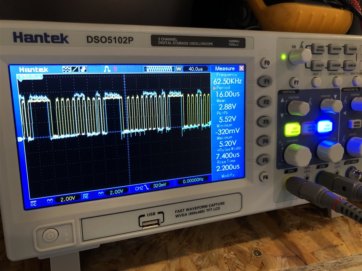
    Now to the most interesting part. I tried to disconnect Ty from Ry on either and both sides. Disconnecting those on the master side did not have any effect. Disconnecting Ty and Ry on the slave side DID have effect. The down-spike totally disappeared. But (as usual), here comes the next problem. Now I see a time skew between SCL and SDA. This time skew is only present on the S side, not R/T side.

    This is a practical problem that again prevents communication because the raise on SDA comes earlier than the SCL drops down. Which apparently makes the slave read one bit as two.

    Please also note that the duty cycle on the SCL is different from 1/2 now.

    I tried to experiment and change a lot of things like:

    * increasing pull-up on the Sx side to make the front less steep. This is the only measure that had occasional effect on communication, but unstable.
    * adding extra capacitance on the Sx side which is essentially the same thing as above.
    * adding extra pull-ups and pull--downs on the TxRx and TyRy on the slave side. With some of these I manage to make the skew worse and with some probably better but not enough to see a difference.
    * connect Ry and Ty with different resistors (just went crazy). Funny: with 300 ohm between Ry and Ty I see both the problems at the same time.
    * swapping TxRx with TyRy on the master side. It was more logical to do this on the slave side but practically I needed to resolder more so I skipped that.

    When I was finished with trying on the HW side I thought that I could actually try to affect timing between SDA and SCL in software on the master itself (Raspberry PI) but this is kind of last resort. Anyway, looking at the original timing on Raspberry PI I wonder why does SDA raise exactly the same moment SCL drops without any margin?

    Just in case, I've got my chips here:

    www.mouser.se/.../P82B96P

    Once again out of ideas :-)

  • Hi Max,

    yes for chance, no for luck (yet). Please, see above.

    Cheers,

    Igor

  • EDIT: (1) changed some grammar mistakes (2) added making SDA pull up resistor weaker on Master side only (3) added in reference targets on I2C spec for rise times (4) added in suggestion for weaker pull up resistor and added cap on TX and SX (slave side)

    Hey Igor,

    "This is a practical problem that again prevents communication because the raise on SDA comes earlier than the SCL drops down. Which apparently makes the slave read one bit as two."

    It looks like your slave device samples data on the falling edge of the clock instead of in the middle of the SCL high period(middle is I2C spec and how its supposed to be done). The other issue I see with this is we are failing to meet the I2C spec as the SDA line is supposed to only change after the SCL line goes below 30%. {for some people this is something that must be met, for others as long as the communication is good then they don't care}

    Assume we want to keep the slave's RY and TY disconnected since it seems to resolve the first problem.

    Here's something we could try:

    I think we could probably try to solve this in hardware by adding a series resistor between the Pull up resistor and the Master's SDA and some capacitance on the master's SDA line. This would change the fall time the master generates because we are now changing the RC constant. I would probably go with something like 50 ohms for the series resistor and maybe ~100pF to ~200pF. This would need to be done only on the SDA master's side (we want a mismatch relative to the Master's SCL). I wouldn't go too crazy with the series resistor because we need to be below ~600mV VoL for the P82B96 to recognize a low. We would probably also want to make the pull up resistor a bit weaker (make it a larger value only on the SDA line) to also make the rise time slower and slow down the propagation [this would also help with our VoL margin]. (for 400kHz we want a rise time faster than 300ns measured from 30% to 70% of Vcc, for 100kHz we want faster than 1microsecond from 30% of Vcc to 70% of Vcc). To add further prop delay on SDA transmission, we can make the pull up resistor  weaker and add capacitance on the slave's Sx side and on the TX tranmission line side as well.

    Another suggestion is to remove the P82B96 on the slave device and resolder a new unit just incase that one was damaged for some reason (maybe ESD related damage? or inductive undershoots on the cable line caused some damage).

    Thanks,

    -Bobby

  • Hi Bobby,

    Here is a fast update on the issue. I didn't have much time to experiment yet.

    Changing P82B96 on both sides I already tried, there is no difference.

    I added the series resistor and capacitor on the master side as you suggested but I didn't see any tangible effect of this. Just to be sure, is it R5+C1 you meant?

      I tried different values up to a combination of 200 pF and 100 Ohm but I didn't see much difference on either side. Because of this I tried some extreme values like 100 Ohm + 5 nF. Then I saw a change but it still wasn't enough for the first data bit and too much for the other. You probably noticed on the oscilloscope images that the first data impulse is longer and supposedly it is the only one which is a problem.  So, moving fronts and changing length of all data impulses ends up fixing one and breaking the other.

    I also tried large capacitance with very large series resistor - 10 nF + 4.7 K but this of course made data impulses unacceptably long. And still not much effect on the front.

    I also tried to increase pull-up resistor on the SDA Sx on master side but I didn't see much difference, maybe because of the series resistor? up to 56 K. Originally it was 4.7 K.   

    I am a bit reluctant changing pull up on the TxRx side because this will supposedly interfere with the amount of slave boards connected (capacitance).

    Now I have another idea: as you may have noticed, the duty cycle on the SCL is not 1/2 after we disconnected Ty and Ry on the slave side. I wonder if there is a way to get it back to 1/2? I am not completely sure but I believe that the problem with "delay" is actually a problem with delayed end of the SCL impulses. If they were 1/2 they supposedly would not overlap with data impulses. What could cause that change in duty cylcle? P82B96 waiting for something on the Ry?

    Just to mention once again that the slave I am using is a standard MCP23017, so I cannot do much about its behavior.   

    Cheers and thanks for help!

    Igor

  • Hi again,

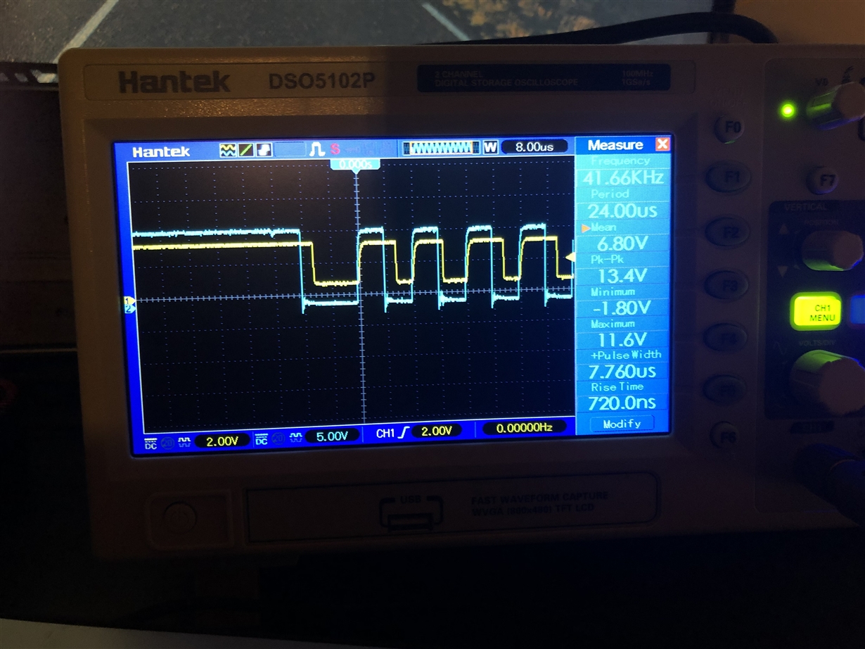
    I checked SCL line on the slave P82B96 on both sides - Ry and Sy and confirmed the fact of changing duty cycle but no delay:

    The yellow one is Sy and the blue one is Ry.

    So far I haven't found a way to affect this other than connecting Ty and Ry which brings back the original problem.

  • Hey Igor,

    Sorry for missing your post, the TI e2e system has tied this thread to Jonathan so I did not receive the update that you posted until I checked manually. (I've assigned myself to this post now)

    It seems something weird is going on with the internal circuit of the device (regarding your last post of the clock signal).

    1) Just to verify, when you disconnected the RX from TX, did you tie a pull up resistor to it or leave it floating? I'm wondering if it wants to see some sort of biasing current equal to the pull up voltage of the TX line.

    2) Just for fun, can you change the Vcc of the device and the pull up voltage from 12V down to 5V?

    In regards to the previous-previous email, we would want C1before R5 though now, I don't think that will do much from what you've tested.

    3) Can you double the side of R3 and R4, but also populate resistors on the slave board on their TX/TY nodes to be the same value as R3/R4 (just for this experiment)

    "I am a bit reluctant changing pull up on the TxRx side because this will supposedly interfere with the amount of slave boards connected (capacitance)"

    Changing the pull ups on that side would just change the rise/fall times. It shouldn't affect the actual capacitance of the slave boards. Adding additional slave boards would add additional capacitance though if you mean by adding pull up resistors on the slaves then I can understand. The IoL on that side would become greater the more boards you put in parallel and could damage the TX/TY drivers of the device (you would be stacking more pull up resistors in series).

    "Now I have another idea: as you may have noticed, the duty cycle on the SCL is not 1/2 after we disconnected Ty and Ry on the slave side. I wonder if there is a way to get it back to 1/2? I am not completely sure but I believe that the problem with "delay" is actually a problem with delayed end of the SCL impulses. If they were 1/2 they supposedly would not overlap with data impulses. What could cause that change in duty cylcle? P82B96 waiting for something on the Ry?"

    I'm not sure why the duty cycle is getting distorted so much here. It looks like the P82B96's propagation delay is changing periodically. The P82B96 should be able to function without the RY pin shorted to the TY pin. Either way, I'll make time next week to see if I can recreate your waveform here in our lab.

    Thanks,

    -Bobby

  • Hi Bobby,

    I have tried everything you suggested above. The only measure that had persistent effect on communication is decreasing the voltage from 12 V to 5 V on the T/R side. When Ty & Ry lines were connected together on both sides the communication went fine. I tried to increase the voltage to see where the threshold is. It is somewhere between 6 and 7 V. 6 V is still fine. 7 V the down-spike is back. 

    If the Ry and Ty lines are disconnected on the slave side (regardless of pull-up on the Ty) the signals look much better at 5 V than 12 V but still not good enough for the slave to start responding.

    Cheers,

    Igor

  • Hi Igor,

    Once again I'm sorry you are having difficulty getting this to work properly, but thank you for all of the detailed information and experimentation.  Bobby is our I2C expert and I am working on creating a duplicate setup to yours based on your description and what boards and DC-DC regulators i have on hand.  We are both thinking about and working on resolving your issues.  I hope to be able to run some tests similar to yours and be able to make some observations on the source of this issue.  I hope to have some results to share with you very soon.

    Regards,

    Jonathan

  • Hi Igor,

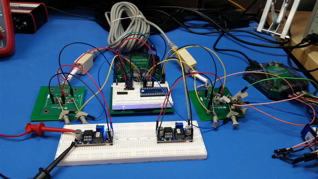
    I have created what I hope to be a functionally equivalent system to yours and unfortunately I am not observing the issues you are describing and my communication and signals appear to be correct.  I'll describe my setup.

    There are couple differences in my setup. 

    1.) I'm using the Analog Discovery 2 module from Digilent as my I2C Master instead of a Raspberry Pi.  If you are not familiar with it, it is a USB multi-function instrument that includes a Protocol Analyzer which I am using for I2C communication as well as other tools such as a Power supply, 2 channel Oscilloscope and Logic Analyzer which are very helpful for debugging a setup. 

    2.) I don't know what your data rate is, but I am running at 100kHz.

    3.) I'm using our 24-Bit IO Expander (TCA6424A) instead of the MCP23S17 you are using as your slave device.

    4.) Instead of a CAT6 cable, I'm using a 25' (7.6m) CAT5E Ethernet Cable that follows the TIA/EIA 568B pinout wiring standard.  I'm using the Green and Blue twisted pairs and the wire colors pin numbers and functions are as follows :

    Pin 1 - White/Orange (Unused)

    Pin 2 - Orange (Unused)

    Pin 3 - White/Green (GND)

    Pin 4 - Blue (SCL)

    Pin 5 - White/Blue (12V VCC)

    Pin 6 - Green (SDA)

    Pin 7 - White/Brown (Unused)

    Pin 8 - Brown (Unused)

    I am using 2 LM2596 DC-DC Buck Switching modules very similar to the ones you showed in a previous post.  I am using the first one to create the 12V rail from a larger rail.  I then could sweep this voltage by adjusting the pot.  The second module takes the 12V from the Slave side of the cable and creates a 3.3V rail to supply the I2C pullup and TCA6424A device.  I will note that I'm using the power supply on the AD2 to create the 3.3V I2C Pullup voltage for the Master I2C signals.  I adjusted the pot on the 12V DC-DC to sweep VCC from 12V to 3.3V and I didn't see any communication loss at any voltage.  So I wasn't able to locate the cause of your voltage dependent behavior.

    I have two small boards that have the P82B96 device, 4.7k ohm pullup resistors to the I2C VCC on Sx/Sy (both Master and Slave boards), and 240 ohm pullup resistors on the Tx/Rx and Ty/Ry lines (Master side only).  These boards have Tx/Rx pins and Ty/Ry pins shorted together at the pins of the device.  I didn't have to separate the pins to get error free communication and my setup essentially follows the application diagram of the datasheet.  I also have a 0.1uF decoupling cap on pin 8 (VCC) and an additional 10uF decoupling capacitor between VCC and GND on the board.  And there is a terminal that I have connected the 4 wires of the Green and Blue twisted pairs of an Ethernet cable. 

    The TCA6424A device is soldered to a 32-pin QFN to DIP breakout board and I'm just using a plastic breadboard for the connections.  It is a simple setup and prone to errors due to the wires and extra parasitic capacitance and inductance due to the wires.  However, I don't appear to be able to duplicate the behavior you are describing.

    Does this match what you are doing?  Or is there something else I am missing that might be critical to your setup that might be critical in solving this issue?  I hope that this might also prompt a thought about what might be different in your setup that will get yours working.

    Can you share any additional details about your setup, the board schematic and layout, cable pin assignments,  data rate, etc. that might help us locate the error?  If you would prefer to not post that information to the forum, but would be willing to share that with me privately, I can look your email address up in the system and reach out to you privately to exchange this information and keep it private.  Just let me know how you would like to proceed.

    Also, we are curious to see what the Cable side (Tx/Rx and Ty/Ry) signals look like.  Could you share some scope shots of those signals?  We are curious about what the Voltage High/Low levels look like as well as the Fall Time and Rise Time measurements between the 70% and 30% levels.  The fall time is more critical and in my setup I am measuring between 10nS and 12nS.  I think every waveform you have shared so far has been on the Sx/Sy side of the device.  I am curious if the duty cycle and skew issues could be the result of the way the signal looks on the 12V side.

    I hope this information is of value to you and hopefully we can figure out what is different in your setup.

    Regards,

    Jonathan

  • Hi Jonathan,

    thank you for your great effort!

    I will scrutinize your set up and compare it with mine. Of course, I was asking myself if I am chasing ghosts like faulty power supply or schematic errors but the thing is I tried different variants of the set up and the behavior stayed persistent no matter what. I started by having a PCB on master side and a similar PCB on the slave side in the field. Then, to confirm my set up I replaced the master side PCB with a breadboard set up still using the same slave PCB. Then eventually I exchanged the slave PCB as well. Thus, there was not a single common HW component between my first set up and my last one. I even tried different brands of P82B96 and they still behaved very similar.

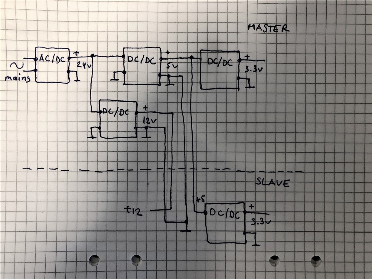
    During my experiments I introduced and removed 3.3 / 5 V logical level converters and 5 -> 3.3 V power supplies, so, maybe, this somehow kept my problem present. Another difference is that I am using more buck converters due to other equipment present in the field but removed for this experiment. My typical power set up on the master side was 24V -> 5V -> 3.3 V (two buck converters in a sequence) plus 24V -> 12V for the P82B96. On the slave side the 12V for the P82B96 is provided from the master side while 5V is received via a separate power rail. On the slave side I have only one buck converter 5V -> 3.3V:

    I have two separate ground rails between master and slave, one with the 5V supply and the other with the 12V supply. This looks strange and error prone and now I don't even remember the exact reason for doing it like that. I believe I wanted to somehow isolate P82B96 from the rest of the system. When I first tried to run this with separated ground lines I experienced a lot of noise on the Sx / Sy side of the P82B96. The noise disappeared once I shorted the ground lines on the slave side (as you see in the picture above) so I kept the two ground lines and kept them shorted. Could this also contribute to the original problem? I am aware of risk for ground loops and possibly other problems but I somehow didn't see any problem with it at that point of time.  

        
    I will come back with hopefully more findings when I've done the comparison.

    Thank you once again!
    Igor    

  • Hi Igor,

    Thanks for the extra information and drawing out the DC voltage tree.  I believe that it isn't possible to have separate grounds between the master and slave notes without using digital isolators since both the master and slave are sharing the same pullup resistors on the Tx/Rx and Ty/Ry pins.  It is possible to galvanically isolate the master and slave by separating the Tx, Rx, Ty, and Ty pins to the isolators, but the ground connection needs to be shared along the cable.

    I have a couple additional questions.

    Are sending both 12V and 5V along the cable in addition to the I2C signals?  Do you need both 5V and 3.3V on the slave board?  If so, this makes sense, but the P82B96 device can operate at either voltage on the I2C bus to match the I2C voltage of the other devices on the bus.

    You've mentioned using 3.3V / 5V Level translators.  Are those on the Master, Slave, or both boards?  Since the P82B96 can operate at either 3.3V or 5V, could you not just set the P82B96 I2C pullup Resistor values to the desired voltage and eliminate the level translators?  I'm curious where they are located in the system and whether or not they are factoring into the errors.  What is the part number of the level translators?  I'm assuming that they are auto-detecting bi-directional translators to handle the SDA data without needing a direction control pin.  My experience with those, are that they have pretty extreme thresholds to detect the High and Low bits and can switch direction easily on noise because they want to quickly change the direction without loosing much of the bit time.  Any sort of reflections or noise in applications with long cables can cause them to switch, and or with signals that fail to reach amplitudes greater than the thresholds.  I have had troubles in the past with these switching directions unexpectedly and the voltage on the opposite side of the translator is passed back onto the bus resulting in errors.  Have you been able to eliminate the possibility that the level translators could be causing any problems?

    Regards,

    Jonathan